4 pinout information, Pinout information, Table 19 – Intel 82540EP User Manual
Page 36
82540EP — Networking Silicon
30
Datasheet
5.4
Pinout Information
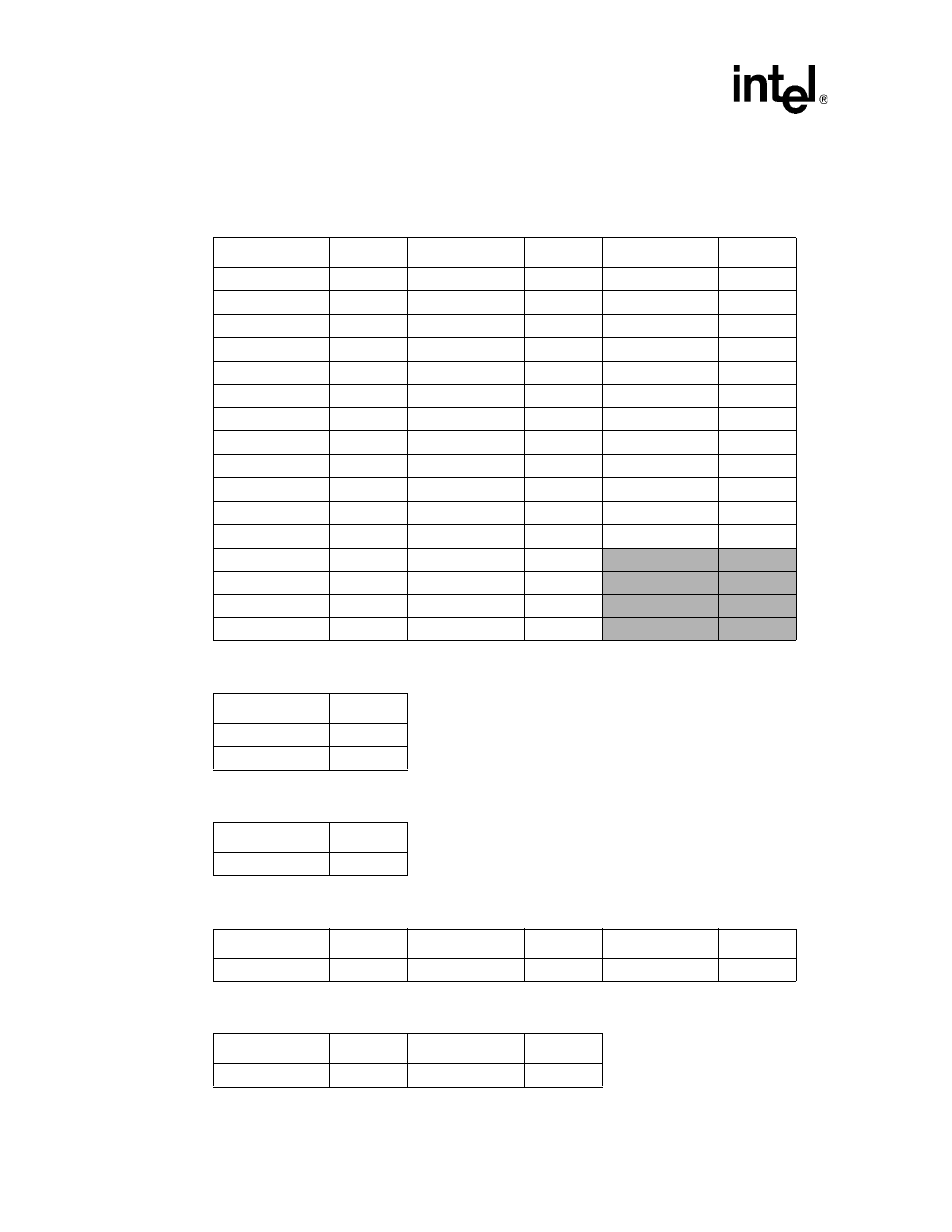
Table 19. PCI Address, Data, and Control Signals
Signal
Pin
Signal
Pin
Signal
Pin
PCI_AD[0]
N7
PCI_AD[16]
K1
CBE0#
M4
PCI_AD[1]
M7
PCI_AD[17]
E3
CBE1#
L3
PCI_AD[2]
P6
PCI_AD[18]
D1
CBE2#
F3
PCI_AD[3]
P5
PCI_AD[19]
D2
CBE3#
C4
PCI_AD[4]
N5
PCI_AD[20]
D3
PAR
J1
PCI_AD[5]
M5
PCI_AD[21]
C1
FRAME#
F2
PCI_AD[6]
P4
PCI_AD[22]
B1
IRDY#
F1
PCI_AD[7]
N4
PCI_AD[23]
B2
TRDY#
G3
PCI_AD[8]
P3
PCI_AD[24]
B4
STOP#
H1
PCI_AD[9]
N3
PCI_AD[25]
A5
DEVSEL#
H3
PCI_AD[10]
N2
PCI_AD[26]
B5
VIO
G2
PCI_AD[11]
M1
PCI_AD[27]
B6
IDSEL
A4
PCI_AD[12]
M2
PCI_AD[28]
C6
PCI_AD[13]
M3
PCI_AD[29]
C7
PCI_AD[14]
L1
PCI_AD[30]
A8
PCI_AD[15]
L2
PCI_AD[31]
B8
Table 20. PCI Arbitration Signals
Signal
Pin
REQ#
C3
GNT#
J3
Table 21. Interrupt Signals
Signal
Pin
INTA#
H2
Table 22. System Signals
Signal
Pin
Signal
Pin
Signal
Pin
CLK
G1
M66EN
C2
RST#
B9
Table 23. Error Reporting Signals
Signal
Pin
Signal
Pin
SERR#
A2
PERR#
J2
- 41210 (64 pages)
- 8xC251TQ (20 pages)
- ENTERPRISE PRINTING SYSTEM (EPS) 4127 (84 pages)
- U3-1L (20 pages)
- 80960HA (104 pages)
- X58 (54 pages)
- ESM-2850 2047285001R (91 pages)
- ATOM US15W (54 pages)
- D915GVWB (4 pages)
- XP-P5CM-GL (28 pages)
- AX965Q (81 pages)
- CORETM 2 DUO MOBILE 320028-001 (42 pages)
- CV700A (63 pages)
- 80C188EA (50 pages)
- X25-M (28 pages)
- XP-P5IM800GV (26 pages)
- IB868 (60 pages)
- D865GVHZ (88 pages)
- IB865 (64 pages)
- Altera P0424-ND (1 page)
- 8086-2 (30 pages)
- IXDP465 (22 pages)
- IWILL P4D (104 pages)
- GA-8I955X PRO (88 pages)
- FSB400 (PC2100) (96 pages)
- D845GLAD (4 pages)
- NAR-3041 (1 page)
- 87C196CA (136 pages)
- G52-M6734XD (74 pages)
- A96134-002 (10 pages)
- Express Routers 9000 (8 pages)
- D865GLC (94 pages)
- IB850 (69 pages)
- MB898RF (62 pages)
- Arima LH500 (78 pages)
- V09 (33 pages)
- I/O Processor (22 pages)
- M600 (110 pages)
- SE7520JR2 (63 pages)
- SERVER BOARD S5520HCT (30 pages)
- Extensible Firmware Interface (1084 pages)
- GA-8IPXDR-E (70 pages)
- D845EBG2 (4 pages)
- AW8D (80 pages)