5 timing specifications, 1 pci bus interface, 1 pci bus interface clock – Intel 82540EP User Manual
Page 28: Timing specifications 4.5.1, Pci bus interface
82540EP — Networking Silicon
22
Datasheet
4.5
Timing Specifications
Note:
Timing specifications are subject to change. Verify with your local Intel sales office that you have
the latest information before finalizing a design.
4.5.1
PCI Bus Interface
4.5.1.1
PCI Bus Interface Clock
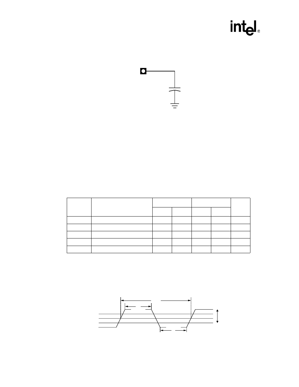
Figure 1. AC Test Loads for General Output Pins
Table 14. PCI Bus Interface Clock Parameters
Symbol
Parameter
a
a. Rise and fall times are specified in terms of the edge rate measured in V/ns. This slew rate must be met across the
minimum peak-to-peak portion of the clock waveform as shown.
PCI 66 MHz
PCI 33 MHz
Units
Min
Max
Min
Max
TCYC
CLK cycle time
15
30
30
ns
TH
CLK high time
6
11
ns
TL
CLK low time
6
11
ns
CLK slew rate
1.5
4
1
4
V/ns
RST# slew rate
b
b. The minimum RST# slew rate applies only to the rising (de-assertion) edge of the reset signal and ensures that system
noise cannot render a monotonic signal to appear bouncing in the switching range.
50
50
mV/ns
CL
Figure 2. PCI Clock Timing
0.6 Vcc
0.2 Vcc
0.5 Vcc
0.4 Vcc
0.3 Vcc
Tcyc
Th
Tl
0.4 Vcc p-to-p
(minimum)
3.3 V Clock