Motorola MVME197LE User Manual
Page 33
Memory Maps
MVME197LE/D2
3-3
3
The memory maps of MVME197LE devices are provided in the following
tables. Table 3-1 is the entire map from $00000000 to $FFFFFFFF. Many areas
of the map are user-programmable, and suggested uses are shown in the table.
This is assuming no address translation is used between the processor and
local peripheral bus and between the local peripheral bus and VMEbus. The
cache inhibit function is programmable in the MC88110. The onboard I/O
space must be marked cache inhibit and serialized in its page table. Table 3-2
further defines the map for the local devices.
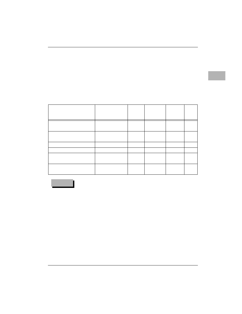
Table 3-1. Processor Bus Memory Map
N
otes
1. This area is user-programmable. The suggested use is
shown in the table. The DRAM decoder is programmed
in the DCAM through the ECDM I
2
CBus interface. The
Processor Bus to Local Peripheral Bus and the Local
Peripheral Bus to Processor Bus decoders are
programmed in the BusSwitch. The Local Peripheral to
VMEbus (master) and VMEbus to Local Peripheral Bus
(slave) decoders are programmed in the VMEchip2.
2. Size is approximate.
3. Cache inhibit depends on devices in area mapped.
4. This area is not decoded. If these locations are accessed
and the local peripheral bus timer is enabled, the cycle
times out and is terminated by a TEA signal.
5. This area is user programmable via the BusSwitch.
Default size is 4 megabytes.
Address
Range
Devices
Accessed
Port
Size
Size
Software
Cache
Inhibit
Notes
$00000000 - (DRAMSIZE -1) User Programmable
(Onboard DRAM)
D64
DRAMSIZE
N
1
DRAMSIZE - $FF7FFFFF
User Programmable
(VMEbus)
D32/D16
3GB
?
2,3
$FF800000 - $FFBFFFFF
Flash Memory
D32
4MB
N
5
$FFC00000 - $FFEFFFFF
reserved
---
3MB
---
4
$FFF00000 - $FFFEFFFF
Local Devices
(Refer to next table)
D32-D8
1MB
Y
---
$FFFF0000 - $FFFFFFFF
User Programmable
(VMEbus A16)
D32/D16
64KB
?
1,3