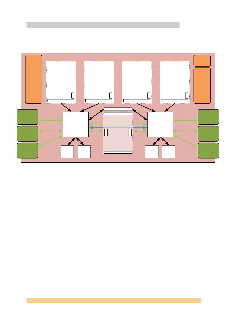
4 data flow block diagram, Figure 10 - data flow diagram – Sundance SMT166 User Manual
Page 27

4.4
Data Flow Block Diagram
Below is shown the block diagram of the board on a data flow point of view and also
showing some of the maximum transfer speed achievable:
SMT166 – SLB Carrier Board
FPGA_0
Virtex 6
LX130T-LX365T
SX315T-SX475T
PSU
Section
DDR3
Memory
Bank 2
4Gbytes/s
SLB
Mezzanine 0
SMT941
SLB
SLB
Mezzanine 1
SMT941
SLB
SLB
Mezzanine 2
SMT941
SLB
SLB
Mezzanine 3
SMT941
SLB
FPGA_1
Virtex 6
LX130T-LX365T
SX315T-SX475T
DDR3
Memory
Bank 3
4Gbytes/s
DDR3
Memory
Bank 0
4Gbytes/s
DDR3
Memory
Bank 1
4Gbytes/s
2
Gbytes
/s
2 Gbytes
/s
2
Gbytes
/s
2 Gbytes
/s
400
Mbytes/s
400
Mbytes/s
800Mbytes/s
2x 2Gbytes/s
PCIe
Cable
x4
800Mbytes/s
Master
Module
SLB Connector
R
S
L
R
S
L
PCIe
Cable
x4
800Mbytes/s
PCIe
Cable
x1
200 Mbytes/s
PCIe
Cable
x1
200 Mbytes/s
USB+CPLD
+Flash
To configure
Virtex6
FPGAs and
access
Master
Module Flash
Clock
Synthesiser
Synchroniser
Top TIM Connector
Bottom TIM Connector
Dual
SATA3.0
500
Mbytes
/s
Dual
SATA3.0
500
Mbytes
/s
Figure 10 - Data Flow Diagram.
The example shown in the above data flow block diagram has been elaborated with
four SMT941s in mind (one of the fastest SLB mezzanine modules within Sundance’s
range with a 2Gbytes/s output rate). SLB data flow can remain ‘local’ and be
processed or stored by the FPGA they are connected to, or be rerouted to the other
FPGA without a slowing down in speed (using channels).
Once stored and processed, data can be transferred at a slower rate to a host.
Product Specification SMT166
Page 27 of 44
Last Edited: 17/06/2014 16:12:00
