Avago Technologies ACPL-P345-000E User Manual
Page 9

For product information and a complete list of distributors, please go to our web site:
www.avagotech.com
Avago, Avago Technologies, and the A logo are trademarks of Avago Technologies in the United States and other countries.
Data subject to change. Copyright © 2005-2013 Avago Technologies. All rights reserved.
AV02-4051EN - May 2, 2013
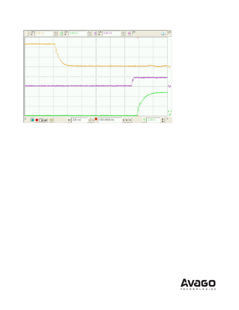
As can be seen from Figure 7 and Figure 8, the turn-off speed of the power MOSFET will be slow, due to the capacitive
effects of D2 and the gate capacitance of Q1. To improve the turn-off speed, the board is provided with a diode resis-
tor pair footprints at D1 and R5 (not mounted NM) to increase the gate current during turn-off. Another way to further
improve the turn-on and turn-off speed is by reducing the gate resistance of R4, but make sure the gate drive current is
not more than 2.5 A.
Figure 8 shows the turn-on signal of IN1+, the turn-on signal at gate of Q1a and the turn-off signal at gate of Q1b.
Figure 8. Turn-on and Turn-off Gate waveforms of Q1a and Q1b
