Avago Technologies ACPL-P345-000E User Manual
Page 4
4
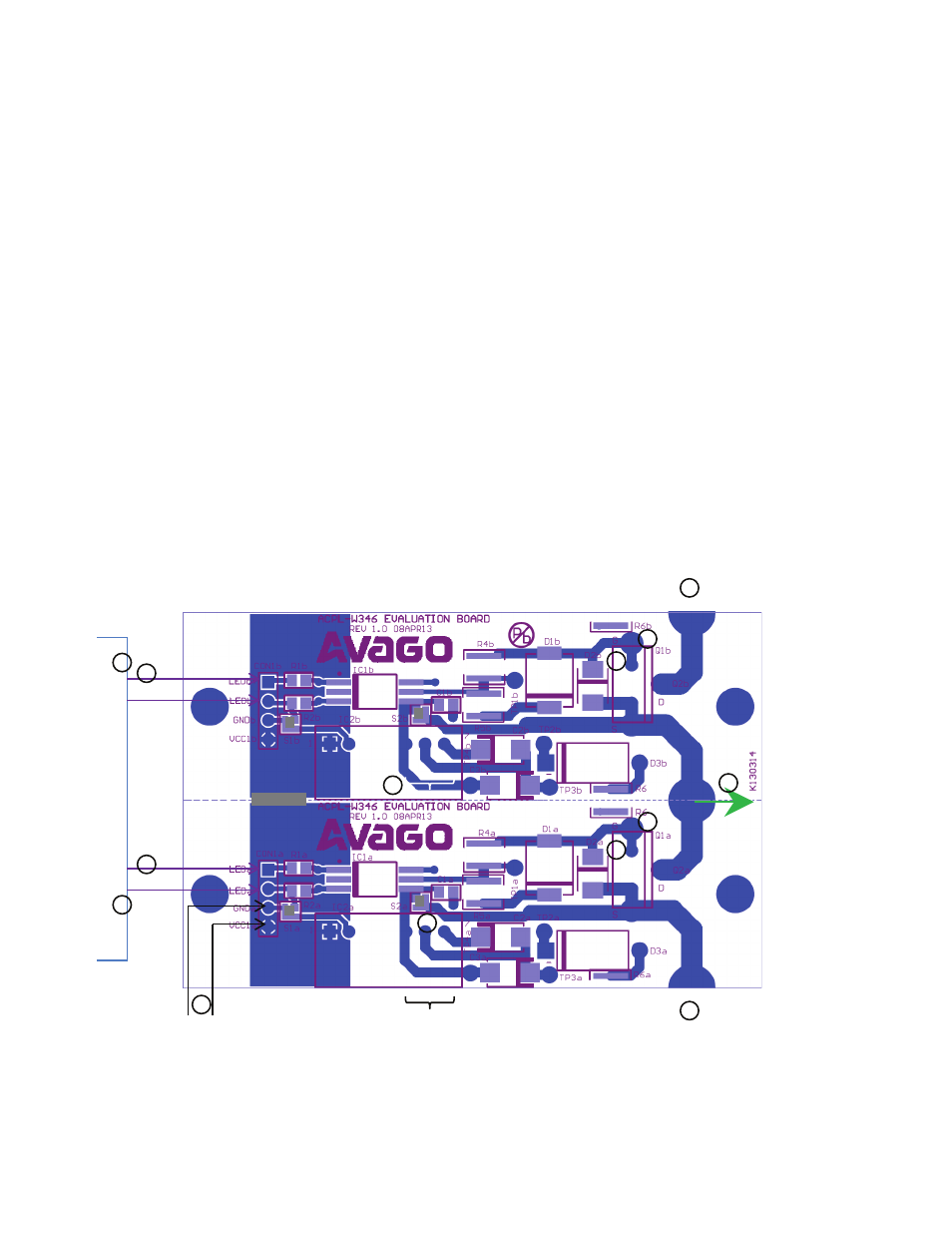
Practical connections of the evaluation board using a power MOSFET for an actual inverter test
1. Solder actual power MOSFETs at Q1 (or Q2) for the top and bottom arms of the half-bridge inverter isolated drivers.
2. Connect a +5V DC isolated supply1 across +5V and GND terminals of CON1 for both arms of the isolated drivers.
3. Connect another isolated DC supply2 (voltage range from 12 V ~ 20 V) across V
CC2a
and V
EEa
at pin 7 and pin 5 of IC2a
respectively for the bottom arm.
4. Connect the signal output (meant to drive the bottom arm of the half-bridge inverter) from the microcontroller to
Signal Input 1 across pin IN1+ and IN1- of CON1a of the bottom inverter arm isolated driver.
5. Connect the signal output (meant to drive the top arm of the half-bridge inverter) from the microcontroller to Signal
Input 2 across pin IN2+ and IN2- of CON1b of the top inverter arm isolated driver. Note: Signal Input 2 should be
180
° out of phase w.r.t. Signal Input 1. Check that V
CC2b
(voltage close to V
CC2a
) is generated through the bootstrap
components D3b and R6.
6. Use a multi-channel digital oscilloscope to capture the waveforms at the following points:
a. LED signal at IN1+ pin w.r.t. GND for the bottom arm.
b. LED signal at IN2+ pin w.r.t. GND for the top arm.
c. Vga for the gate driving voltage of Q1a (or Q2a) w.r.t. V
Ea
of the bottom inverter arm (differential probe needed).
d. Vgb for the gate driving voltage of Q1b (or Q2b) w.r.t. V
Eb
of the top inverter arm (differential probe needed).
7. Connect a power cable from the output pin (marked Load) to the inverter load.
8. Connect the high voltage cables from the top arm power MOSFET drain pin to HVDC+ and from the bottom arm
power MOSFET source pin to HVDC-, respectively, as shown. (Note: It is recommended that you enable the current-
limiting function of the HV power source supplying the high voltage DC bus voltage during this test to protect the
inverter and its driver circuitries).
Microcontroller
IN1+
IN1- Signal Input 1
+5V
GND
DC Supply1
IN2+
IN2- Signal Input 2
Power
MOSFET
mounted
1
1
2
3
12~20 V
+
DC Supply2
4
5
12~20V
+
5
6a
6b
6c
6d
Load
7
HVDC+
HVDC
–
8
8
–
–
Power
MOSFET
mounted
Figure 4. Connection of evaluation board in actual applications