Avago Technologies ACPL-P345-000E User Manual
Page 8
8
Figure 7. Turn-off and Turn-on Gate waveforms of Q1a and Q1b
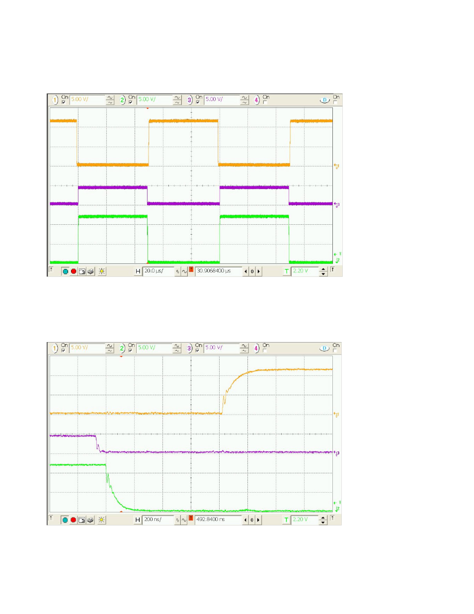
Figure 6. Input LED signal and Power MOSFET Gate Voltage Waveforms
Figure 6 also shows that, once a bootstrap supply is adopted, the amplitude of the output voltage at the top inverter arm
will be slightly smaller than that of the bottom inverter arm, at 180
° out of phase. (IN1+ is set at 49% duty ratio, while
IN2+ (not shown) is also set with 49% duty ratio, plus a turn-on delay of 100 ns with respect to IN1+).
Figure 7 shows the turn-off signal of IN1+, the turn-off signal at gate of Q1a, and the turn-on signal at gate of Q1b.
Output Measurement
A sample of input LED and various output waveforms are captured and shown in Figure 6. The default setup connection
is adopted, except with Q1a and Q1b power MOSFETs are mounted. The power MOSFETs used have a gate capacitance
equivalent to 10 nF.