Chapter 6 digital lines, Warning – Remote Processing RPC-150 User Manual
Page 17
CHAPTER 6
DIGITAL LINES
RPC-150
Page 15
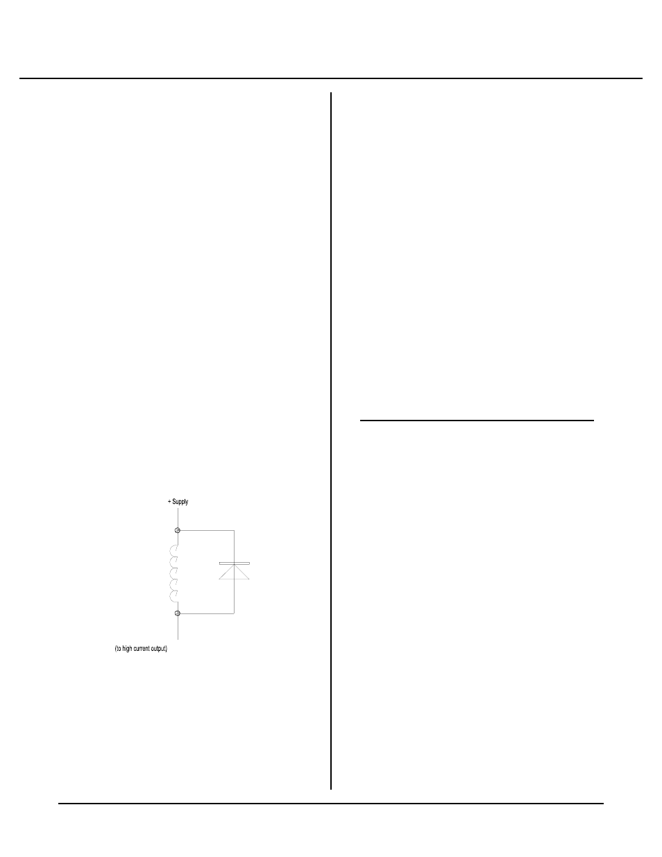
Figure 6-2 Inductive load protection
The output driver chip, U 13, can be replaced w ith a DIP
shunt jumper so it is like the other lines at J2. Install the
jumper so U13 pin 1 goes to pin 18.
NOTE: Outputs at the high current lines are not
compa tible with TT L logic leve ls and should
not be used to drive other logic devices.
Each of the high current outputs can sink 100 ma at 50V.
WARNING:
External supplies using the high cu rrent outputs m ust
be tied to J2, pin 26 and NOT the power connector.
Failure to do so can produce a ground loop and
cause erratic operation.
The ther mal time constant of the p ackage is ve ry shor t,
s o th e nu m b er o f o u tp u ts th a t a r e on a t a n y o n e t im e
should include those that overlap even for a few
milliseconds.
Incandesc ent lamps h ave a " cold" c urre nt of 11 times its
o p er a ti ng c ur r e nt . L a m ps r eq u ir i ng m o re th a n 5 0 m a
should not be used.
Protection diodes m ust be used with inductive loads.
Refer to figure 6-2
Do not pa rallel outputs f or higher drive. This could
result in damage since outputs will not share current
equally.
Interfacing to an opto-module rack
J2 and J3 I/O lines can be interfaced to an MPS-8, 16,
or 24 position opto module rack. Lines not going to an
opto module connect to a screw terminal on the MP S-
XX series boards. This feature allows you to connect
s w it ch e s o r ot he r T T L t yp e de v ic e s t o t he d ig it al I/ O
lines. The MPS-XX series boards accept G4 series
modules.
Use the O PTO comm and to acces s and contr ol G4 opto
modules. The LIN E comm and is used to access
individual lines on the STB-26 or MPS-X X board.
A CM A-26 connects J2 and J3 on the RPC-150 to the
MPS-XX board. Cable length should be less than 2 feet
for the 8 position rack and 18 inches for the 16 and 24
positions. Excessive cable lengths cause a high voltage
drop and consequently unreliable operation. Connect
+ 5V and gro und to the opto racks.
You must configure the 8255 ports for outputs using the
CON FIG PIO sta tement. Use the follo wing table to
determine the corresponding opto channel for a
particular 82C55 p ort:
Opto
82C55
Connector
Addr.
channels
port
M100-M 103
Lower C
J2
514
M104-M 107
Upper C
J2
514
M108-M 115
A
J2
512
M116-M 122
B
J2
513
M123
not available
M0-M 3
Lower C
J3
2
M4-M 7
Upper C
J3
2
M8-M 15
B
J3
1
M16-M 23
A
J3
0
"Opto channel" is the position as marked on the MP S-xx
board. The channel number is preceded by a ' M'
character on the MPS board. W hen connecting J2 to an
opto rack, add 100 to the number on the rack. J2 has a
high current output on port B (channels M8-M15).
Replace U13 with a shunt jumper to operate norm ally.
You will have to group your inputs and outputs on the
rack to make best use of the space. See D i gi ta l I / O
Program ming Ex ample later in this chapter for
information about using these commands. P ay attention
to how LINE differs from OP TO in addressing and
polarity.
To turn on an opto module, an output line must be low.
A mod ule is turned off by wr iting a ' 1' to a channel.