Digital lines chapter 6 – Remote Processing RPC-150 User Manual
Page 16
DIGITAL LINES
CHAPTER 6
Page 14
RPC-150
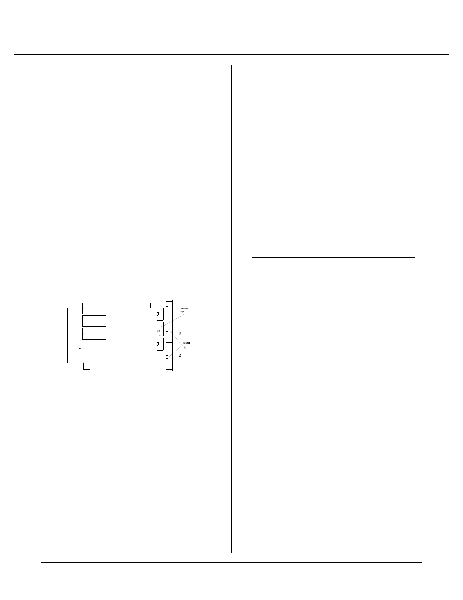
Figure 6-1 Digital I/O
INTRODUCTION
Digital I/ O lines ar e used to inter face with op to-module
racks, switches, low current LED's, and other TTL
devices. The RP C-150 h as 47 of these line s available
through J2 and J3. Seven of these lines are high current
outputs, capable of sinking 75 to 200 ma. Eight lines on
J2 are shared by the keypad connector, J5. When the
keypad is used, 8 of the 47 lines are not available.
Eight, 16, or 24 position opto racks are connected to J2
or J3. These opto rac ks accept G4 ser ies opto modules.
G4 series opto modules are used to sense the presence of
AC or D C voltages or switch them. Maximum
switching curr ent is 3 ampere s.
WARNING:
Apply power to the RPC -150 before applying a
voltage to the digital I/O lines to prevent current
from flowing in and damaging devices. If you
cannot apply power to the RPC-150 first, contact
technical support for suggestions appropriate to your
application.
DIGITAL I/O PORT
Digital I/O lines on the RPC-150 are supplied by an
82C55 chip. T he chip' s lines go to connectors J2 and
J3.
The lines on J2 and J3 ar e divided into 3 eig ht bit
groups. P orts A and B can be configured as all inputs or
outputs. Port C can be programm ed as one group of 8
inputs or outputs or as two groups of four lines (upper
and lower C). T he four lines in upper and lower C can
each be pr ogram med as a ll inputs or outp uts. P ort B, bit
7 on J2 mu st be used as an output.
When a line is configured as an output, it can sink a
m a x im u m o f 2 . 5 m a a t 0 . 4 V an d ca n so u r ce o ve r 2 . 5 m a
at 2.4V. Outputs sink 15 ma at 1.0V.
J2 and J3 are accessed using CAMBASIC LINE, OPTO,
INP, and OUT statements. LINE r eads or writes to a
port based on the connector pin number. OPTO reads or
writes to an opto module based on its position in an MPS
opto rack . IN P and O UT a ccess a byte o f data at a por t.
The base address for J2 is 512 and J3 is 0 when using
CON FIG PIO , IN P, and OUT statements. CON FIG
PIO statement is used to configure the 8255 lines. Upon
reset, lines are configured for inputs. Use CO NFIG PIO
to configure lines for outputs and inputs.
J2 and J3 ar e accessed using LIN E or O PTO statements
according to the table below.
Connector
LINE #
OPTO r ack
N o
terminal
position
J3
1 - 25
0 - 23
J2
101 - 124
100 - 122
J2 port B is connected to a high current sink through
U13. See " High current output" later in this chapter.
Line 107 is not available.
J2 port C is shared with the keypad port J5. If you are
using a keypad through J5, these 8 lines are not
available.
Pull up resistors
Digital I/ O lines at J2 an d J3 are p ulled up to + 5 volts
through a 10K resistor pack.
These pull ups makes interfacing to switches and "open
collector" TTL devices easy . See "Inter facing to
Switches and other devices" below.
High current output
Eight lines at J2 can be used as high cur rent driver s.
These outputs will switch loads to ground. Outputs are
controlled by Port B on the 82C55. Its address is 513.
Port B bits 0- 6 are use d to contro l the high cur rent por t.
Logic outputs from this port are inverted. That is, when
a 1 is writte n to the high cur rent por t, the o utput is
switched on and goes low.