Chapter 3, Motherboard information – Lanner FW-8759 User Manual
Page 22
16
Motherboard Information
Network Application Platforms
Chapter 3
Clear CMOS and Disable ME Jumper Setting (J4): It
is for clearing the CMOS memory and system setup
parameters by erasing the data stored in the CMOS
RAM such as the system passwords. The ME_disable
setting allows updating the Intel Management
Engine firmware through software without a
electronic programmer. The Intel ME's leverage of
non-volatile storage prevents users from removing
critical inventory, remote control, or virus protection
agents.
To clear CMOS, disconnect AC power supply. Set the
jumper to 4-6 and wait a minute to be sure the
CMOS has been cleared. Then return the CMOS
jumper to it's original position.Restore power to the
system.
Bypass LED Function (J12)
Generation 3 Bypass Firmware Download Connector
(J7)
Generation 3 Bypass Program Selection Header (J8)
Hardware or Software Reset Jumper(J3): The jumper can
be adjusted to be in either hardware or software reset
mode when the reset switch is pressed. The hardware
reset will reboot the system without turning off the
power. The software reset can be programmed to
reset a software to its default setting.
ATX Power Connector(ATX1, ATX2): Find the proper
orientation when inserting the plugs, for the supply
plugs are designed to fit these connectors in only one
orientation.
AT/ATX Mode Selection Header (J13)
AT Mode Power Connector (CONN5)
Onboard Power-on Tact Switch(SW2)
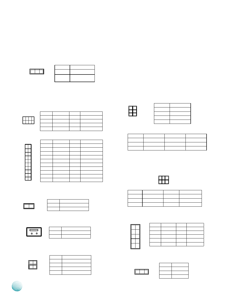
Pin No.
Signal
Pin No.
Signal
1
GND
2
+12V
3
GND
4
+12V
5
GND
6
+12V
7
GND
8
+12V
Pin No.
Function
1-2
HW Reset
2-3
Software Reset
(default)
1
2
7
8
20
2
19
1
Pin No.
Signal
Pin No.
Signal
1
+3.3V
2
+3.3V
3
+3.3V
4
-12V
5
GND
6
GND
7
+5V
8
PSON
9
GND
10
GND
11
+5V
12
GND
13
GND
12
GND
15
PROK
16
-5V
17
5VSB
18
+5V
19
+12V
20
+5V
3 2 1
1 2
Pin No.
Signal
1
P3V3
2
MR#
3 1
4 2
Pin No.
Signal
1
GND
2
GND
3
PWR_BTIN_N
4
PWR_BTIN_N
Pin No.
Signal
1
GND
2
PSON-
2 1
1
3
5
2
4
6
Pin No.
Function
1-3
ME_DISABLE
3-5
NORMAL
2-4
NORMAL
4-6
CLEAR CMOS
9
1
10
2
Pin No. Function Pin No.
Function
1
NC
2
NC
3
NXP_RXD
4
NXP_RTS_N
5
NXP_TXD
6
NXP_CTS_N
7
NC
8
NC
9
GND
10
P3V3SB
Pin No.
Signal
Pin No.
Signal
1
CPLD_LED1_L
2
CPLD_LED1
2
CPLD_LED2_L
4
CPLD_LED2
3
CPLD_LED3_L
6
CPLD_LED3
2 6
1 5
Pin No.
Function
1
P3V3SB
2
CPLD_LED3
3
GND
1 2 3
Pin No.
Signal
Pin No.
Signal
1
P3V3SB
2
NC
3
ME_DISABLE
4
RTCRST#
5
NC
6
GND