Chapter 3: motherboard information, Block diagram, Chapter 3 – Lanner FW-5330 User Manual
Page 10: Motherboard information, Mb-5330
7
Motherboard Information
Chapter 3
Network Application Platforms
Chapter 3:
Motherboard Information
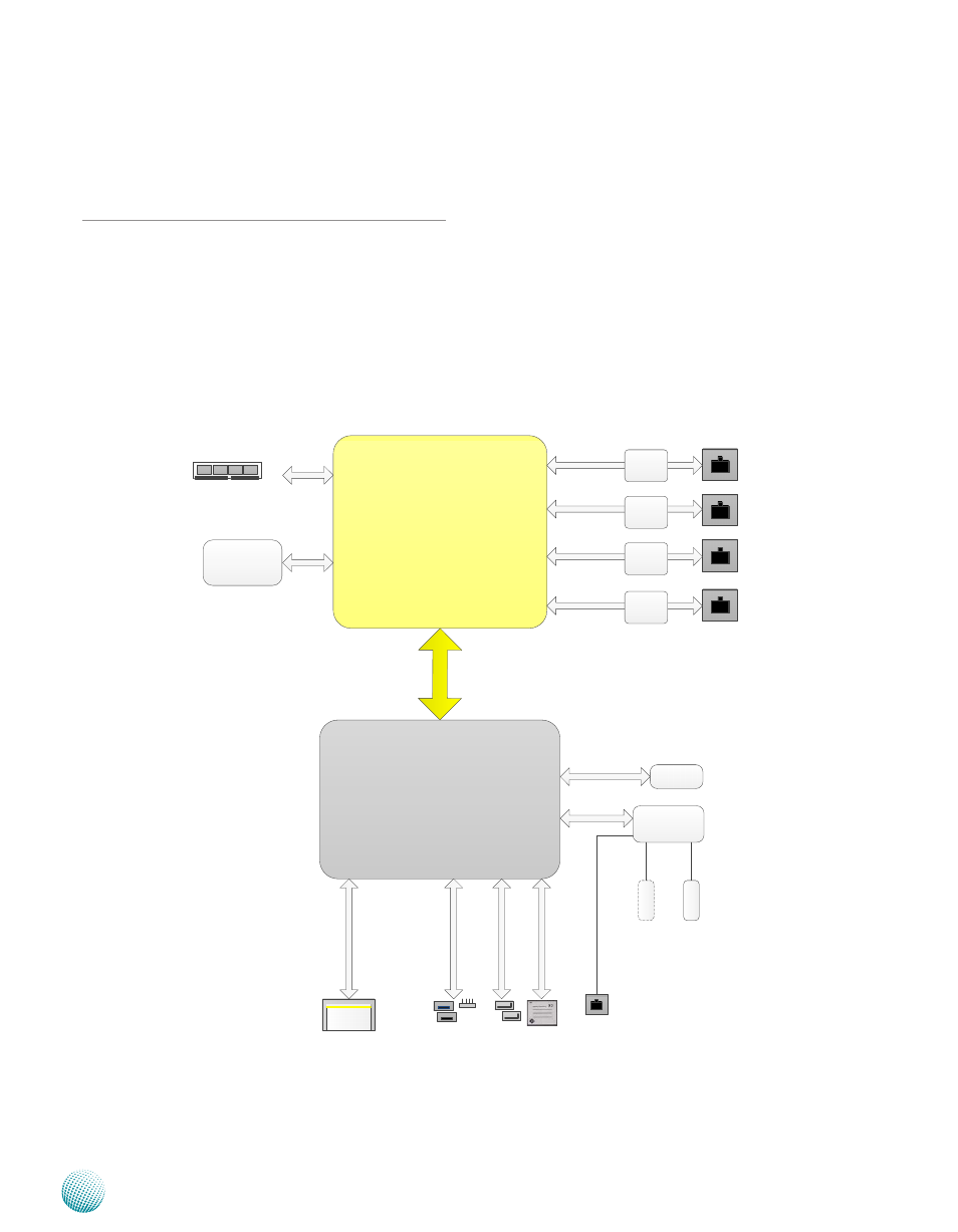
Block Diagram
The block diagram depicts the relationships among the
interfaces or modules on the motherboard. Please refer
to the following figure for your motherboard’s layout
design.
AMD
A50M
Controller Hub
AMD G-Series APU
T24L (5W)
T40R (5.5W)
T40E (6.4W)
1 x DDR3 1066 SO-DIMM
UMI
PCIe x1
PCIe x1
PCIe x1
PCIe x1
VGA pin header
(Reserved for
other CPU)
1
x
SA
TA
6
Gb
/s
2
x
U
SB
2
.0
C
on
ne
ct
or
1
x
U
SB
2
.0
p
in
h
ea
de
r
1
x
PC
Ie
x1
PCIe x1 USB
SATA
SPI
8MB
Winbond
83627DHG-P
LP
C
SP
I
K/
M
RJ45 Console
LC
M
CF
SATA CF
SATA
MB-5330
PCIe x1
PCIe x1
mini PCIe
connector
1
x
PC
Ie
x1
Realtek
RTL8111E
Realtek
RTL8111E
Realtek
RTL8111E
Realtek
RTL8111E
Reserved
for customization
See also other documents in the category Lanner Computer hardware:
- LVC-2000 (39 pages)
- LVC-5000(N4) (42 pages)
- LVC-5550S (41 pages)
- LVC-5570 (48 pages)
- LVC-5770 (49 pages)
- FW-6432 (16 pages)
- FW-7525 (41 pages)
- FW-6486 (18 pages)
- FW-6436 (19 pages)
- FW-7573 (44 pages)
- FW-7568 (52 pages)
- FW-7540 (47 pages)
- FW-8759 (47 pages)
- FW-7581 (23 pages)
- FW-8758 (42 pages)
- FW-7610 (44 pages)
- FW-8756 (24 pages)
- FW-7575 (48 pages)
- FW-8760 (53 pages)
- FW-8877 (46 pages)
- FW-8892 (58 pages)
- FW-8893C (49 pages)
- FX-3411 (48 pages)
- FW-8894 (31 pages)
- FW-8771 (47 pages)
- RS12-38800 (64 pages)
- MR-320 (20 pages)
- FX-3210 (54 pages)
- MR-301 (16 pages)
- MR-350 (12 pages)
- MR-330A (16 pages)
- MR-730 (18 pages)
- VES-220 (19 pages)
- VES-270 (19 pages)
- VES-310 (15 pages)
- VES-310 V2 (20 pages)
- VES-500 (21 pages)
- EM-F345 (30 pages)
- VES-8X2 (16 pages)
- VES-8X6 (17 pages)
- LEC-2026 (67 pages)
- LEC-2010 (65 pages)
- LEC-2136 (20 pages)
- LEC-2050 (38 pages)