Global bus, Led setting, Led register dsp-a – Sundance SMT374 User Manual
Page 14: Led register dsp-b
Version 2.2
Page 14 of 29
SMT374 User Manual
The addresses of the SDB registers are shown in the
described in the
Note that TI’s C6713 processors are unable to move data fast enough to use the full
bandwidth of 32-bit SDBs. Observed maximum transfer rates using EDMA are
340MB/s (internal memory) and 130MB/s (external memory). TI claims a potential
bandwidth of 400MB/s. This is currently under investigation.
Global bus
The SMT374 provides a single global bus interface. This is only accessible from
DSP-A. The addresses of the global bus registers are shown in the
, and are described in the
LED Setting
The SMT374 has 5 LEDs. One shows the FPGA configuration status and the other 4
are under DSP control (2 each).
Two output TTL I/O pins are available on connector JP2 for control or debugging.
Their values can be controlled by bits in the LED register.
LED D2 always displays the state of the FPGA DONE pin. This LED is off when the
FPGA is configured (DONE=1) and on when it is not configured (DONE=0).
This LED should go on when the board is first powered up and go off when the FPGA
has been successfully programmed (this is the standard operation of the boot code
resident in the flash memory device). If the LED does not light at power-on, check
that you have the mounting pillars and screws fitted properly. If it stays on, the DSP
is not booting correctly, or is set to boot in a non-standard way.
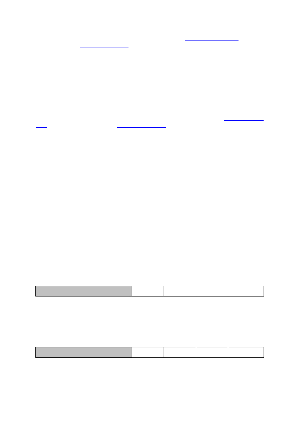
LED Register DSP-A
(0xB00D0000)
31–4
3 2 1 0
TTL1
TTL0
LED D4
LED D3
RW,0 RW,0 RW,0 RW,0
LED Register DSP-B
(0xB00D0000)
31–4
3 2 1 0
TTL3
TTL2
LED D6
LED D5
RW,0 RW,0 RW,0 RW,0