Timer, Timer control register – Sundance SMT363XC2 User Manual
Page 16
Version 2.2
Page 16 of 27
SMT363XC2 User Manual
Timer
The TIM TCLK0 and TCLK1 signals can be routed to the DSP’s TOUT/TINP pins.
The signal direction must be specified, together with the routing information in the
timer control register.
Timer Control Register
31–6 5
4
3–0
Reserved
TCLK1 TCLK0 Reserved
Field Description
0 TIM TCLK0 is an input
TCLK0
1 Enable TIM TCLK0 as an output
0 TIM TCLK1 is an input
TCLK1
1 Enable TIM TCLK1 as an output
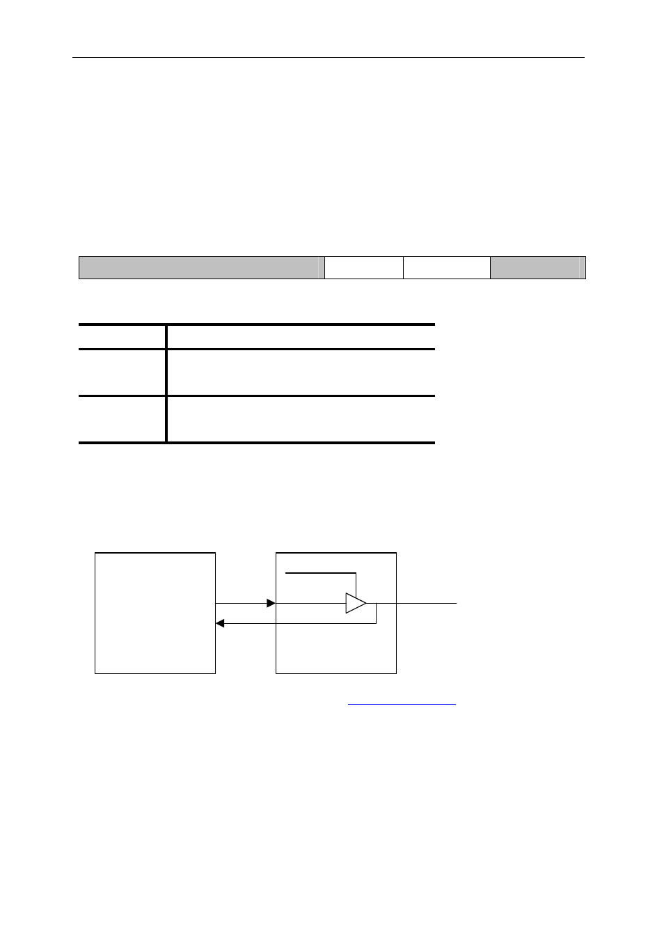
If the TIM TCLKx pin is selected as an output, the DSP TOUTx signal will be used to
drive it. The TIM TCLKx pin will always drive the DSP TINPx input.
C6x
FPGA
TOUT0
TINP0
TCLK0EN
TCLK0
The Timer control register is described in the
See also other documents in the category Sundance Equipment:
- SMT107 (16 pages)
- SMT6035 v.2.2 (39 pages)
- SMT6012 v.4.6 (22 pages)
- FC100 (12 pages)
- FC108 v.1.1 (10 pages)
- SMT6065 v.4.0 (45 pages)
- FFT v.2.1 (19 pages)
- SMT111 (18 pages)
- SMT118LT (10 pages)
- SMT118 (20 pages)
- SMT123-SHB (13 pages)
- SMT128 (15 pages)
- SMT145 (18 pages)
- SMT148 (35 pages)
- SMT130 v.1.0 (46 pages)
- SMT148FX (48 pages)
- SMT310Q (55 pages)
- PARS (70 pages)
- SMT166-FMC (52 pages)
- SMT166 (44 pages)
- SMT300Q v.1.6 (61 pages)
- SMT310 v.1.6 (50 pages)
- SMT317 (24 pages)
- SMT326v2 (24 pages)
- SMT338 (19 pages)
- SMT349 (32 pages)
- SMT339 v.1.3 (27 pages)
- SMT338-VP (22 pages)
- SMT358 (25 pages)
- SMT351T (37 pages)
- SMT351 (25 pages)
- SMT350 (45 pages)
- SMT362 (30 pages)
- SMT365G (23 pages)
- SMT364 (37 pages)
- SMT373 (15 pages)
- SMT368 (24 pages)
- SMT370v3 (46 pages)
- SMT377 (22 pages)
- SMT381 2007 (31 pages)
- SMT381-VP (81 pages)
- SMT387 (42 pages)
- SMT391 (18 pages)
- SMT384 (47 pages)
- SMT390-VP (55 pages)