Led control, Codec interface fpga – Sundance SMT326v2 User Manual
Page 8
Release
Page 8 of 24
SMT326 DSP PC/ISA System User Guide
Document Name:
SMT326 Ugv2.doc
Original Date: 08/11/97
Product Name:
SMT326
Revision Date: 08/26/99
Author:
Graeme Parker – Fabio Ancona
LED Control
An 8 bit latch is provided within the Codec FPGA to enable the state of an on board hex LED
to be changed. The LED is controlled by the 4 lsbs of this register. This register is accessed
at address 0x80200020.
The next 3 msbs of this register select which of the CODECs are selected for configuration
via the I
2
C interface device.
The msb of this register is used to reset the CODECs. A logic 1 will remove the reset signal.
Global Memory Interface Control Register (GMICR)
Within the 'C44 is a register which determines how the bus is partitioned and how many wait
states to use for accesses.
The value 0x34F4F840 must be programmed into the GMICR. When using an operating
system like 3L, the loading of this register is performed using the value within the ID ROM.
This value will provide 0 wait state access to SRAM (external ready), externally defined wait
states for access to the I2C interface, and n wait states for access to the CODECs.
Codec Interface FPGA
The XC4006 FPGA is configured by the ‘C44. Normally this is done by ‘C44 boot code
resident within the boot ROM. This code would read the spare section of the ID ROM and
use this as configuration data for the FPGA.
The FPGA is configured in a byte wide asynchronous peripheral mode. The PROGRAM pin
is asserted by the ‘C44 writing to address 0x80300000. This pin is de-asserted when address
0x803000000 is read.
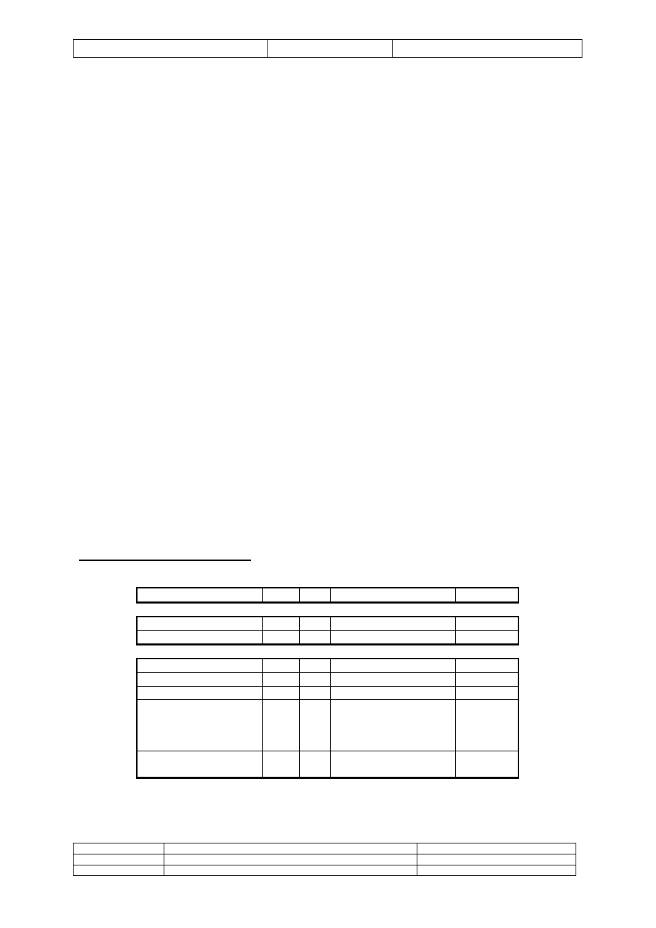
C44 Memory Map Summary
Address
A20
A4
Function
Strobe
(00)30 0000
Local SRAM
LSTRB0
(70)00 0000
ID ROM
LSTRB0
(80)00 0000
0
x
Global SRAM
STRB0
(80)10 0000
1
x
I
2
C
STRB1
(80)20 0000+nn
0
0
ADC/DAC nn
STRB1
(80)20 0020
0
1
W:LED & I
2
C control
R:Status,
bit 0 - interrupt status
bit 1 - left/right status
STRB1
(80)30 0000
1
x
W: Set FPGA PROG
R: Clr FPGA PROG
STRB1