Iiof connectivity, Fpga configuration, Iiof connectivity fpga configuration – Sundance SMT148 User Manual
Page 18
Version 1.4
Page 18 of 35
SMT148 User Manual
IIOF Connectivity
Each TIM site provides 3 interrupt pins, IIOF0, 1 & 2.
IIOF0 & 1 are connected in a daisy-chain with TIM site 1 IIOF0 connected to TIM site
2 IIOF1; TIM site 2 IIOF0 connected to TIM site 3 IIOF1 finishing with TIM site 4
IIOF0 connected to TIM site 1 IIOF1.
All TIM site’s IIOF2 signals are connected together.
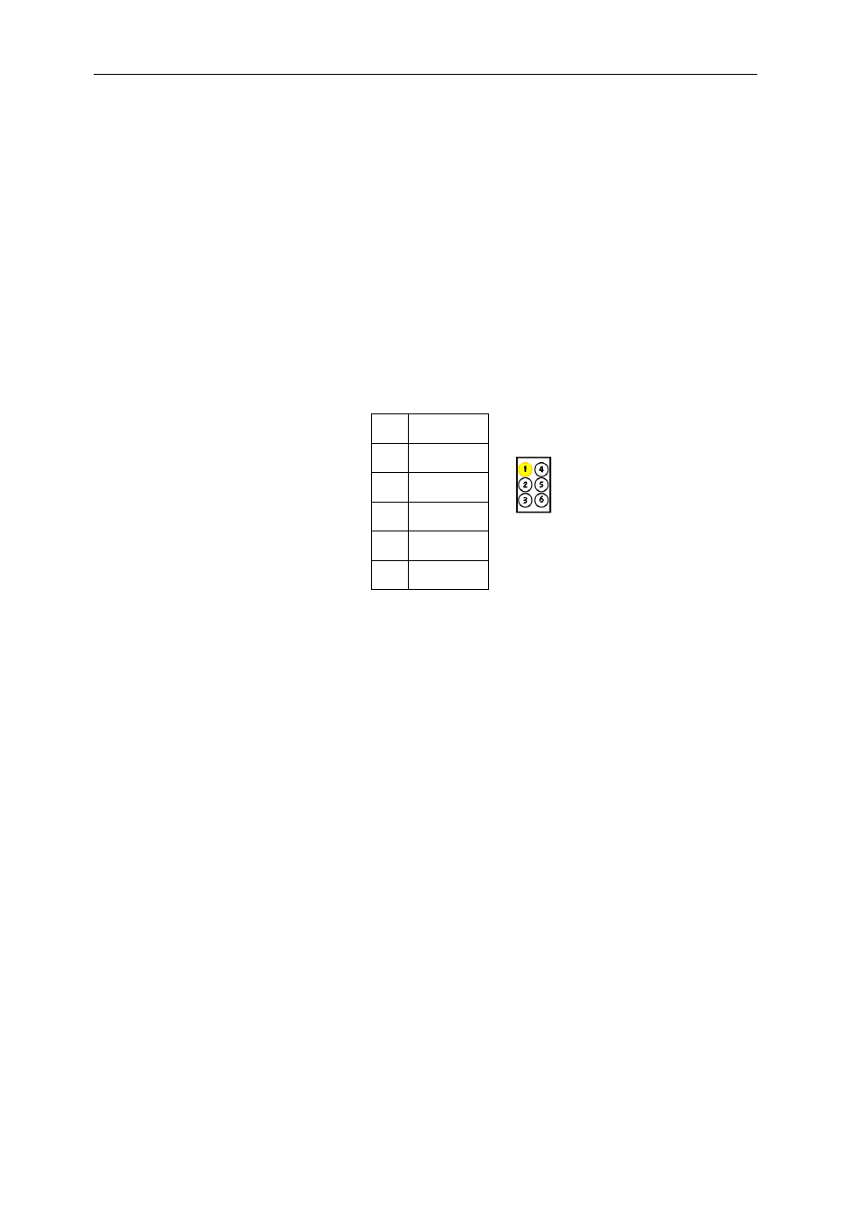
FPGA configuration
In the default configuration the FPGA is configured by the microcontroller that fetches
the configuration in the flash device. However it is possible to download a new
configuration to the FPGA using the Xilinx JTAG cable connected to a PC and to JP5
on the SMT148 carrier. The pinout is as follow:
1 3.3V
2 GND
3 TMS
4 TCK
5 TDI
6 TDO
Table 13 : FPGA configuration
- SMT107 (16 pages)
- SMT6035 v.2.2 (39 pages)
- SMT6012 v.4.6 (22 pages)
- FC100 (12 pages)
- FC108 v.1.1 (10 pages)
- SMT6065 v.4.0 (45 pages)
- FFT v.2.1 (19 pages)
- SMT111 (18 pages)
- SMT118LT (10 pages)
- SMT118 (20 pages)
- SMT123-SHB (13 pages)
- SMT128 (15 pages)
- SMT145 (18 pages)
- SMT130 v.1.0 (46 pages)
- SMT148FX (48 pages)
- SMT310Q (55 pages)
- PARS (70 pages)
- SMT166-FMC (52 pages)
- SMT166 (44 pages)
- SMT300Q v.1.6 (61 pages)
- SMT310 v.1.6 (50 pages)
- SMT317 (24 pages)
- SMT326v2 (24 pages)
- SMT338 (19 pages)
- SMT349 (32 pages)
- SMT339 v.1.3 (27 pages)
- SMT338-VP (22 pages)
- SMT358 (25 pages)
- SMT351T (37 pages)
- SMT351 (25 pages)
- SMT350 (45 pages)
- SMT362 (30 pages)
- SMT365G (23 pages)
- SMT364 (37 pages)
- SMT373 (15 pages)
- SMT368 (24 pages)
- SMT370v3 (46 pages)
- SMT377 (22 pages)
- SMT381 2007 (31 pages)
- SMT381-VP (81 pages)
- SMT387 (42 pages)
- SMT391 (18 pages)
- SMT384 (47 pages)
- SMT390-VP (55 pages)