Lvds drivers/receivers – Sundance SMT148 User Manual
Page 12
Version 1.4
Page 12 of 35
SMT148 User Manual
LVDS drivers/receivers
24 LVDS drivers and 24 LVDS receivers are fitted on the carrier card to convert
LVDS signals from/to LVTTL signals. The connectors used for the LVDS signals are
four straight
(191-037-113-001). In the default carrier FPGA
firmware implementation two McBSP connections coming from each TIM site are
mapped per connector.
1 GND Input/Output
20 GND
2 McBSP_CLKR_Tx_0+
I
21 McBSP_CLKR_Tx_0-
3 McBSP_FSR_Tx_0+
I
22 McBSP_FSR_Tx_0-
4 McBSP_DR_Tx_0+
I
23 McBSP_DR_Tx_0-
5 GND
24 GND
6 McBSP_CLKX_Tx_0+
O
25 McBSP_CLKX_Tx_0-
7 McBSP_FSX_Tx_0+
O
26 McBSP_FSX_Tx_0-
8 McBSP_DX_Tx_0+
O
27 McBSP_DX_Tx_0-
9 GND
28 GND
10 GND
11 GND
29 GND
12 McBSP_CLKR_Tx_1+
I
30 McBSP_CLKR_Tx_1-
13 McBSP_FSR_Tx_1+
I
31 McBSP_FSR_Tx_1-
14 McBSP_DR_Tx_1+
I
32 McBSP_DR_Tx_1-
15 GND
33 GND
16 McBSP_CLKX_Tx_1+
O
34 McBSP_CLKX_Tx_1-
17 McBSP_FSX_Tx_1+
O
35 McBSP_FSX_Tx_1-
18 McBSP_DX_Tx_1+
O
36 McBSP_DX_Tx_1-
19 GND
37 GND
Table 4: LVDS pinout (default firmware)
x refers to the TIM site number.
Each LVDS input pair is terminated with a 100Ω resistor. The LVDS driver devices
are enabled by a signal generated by the FPGA (TX_EN), each enable controls 2
McBSP ports (see firmware description).
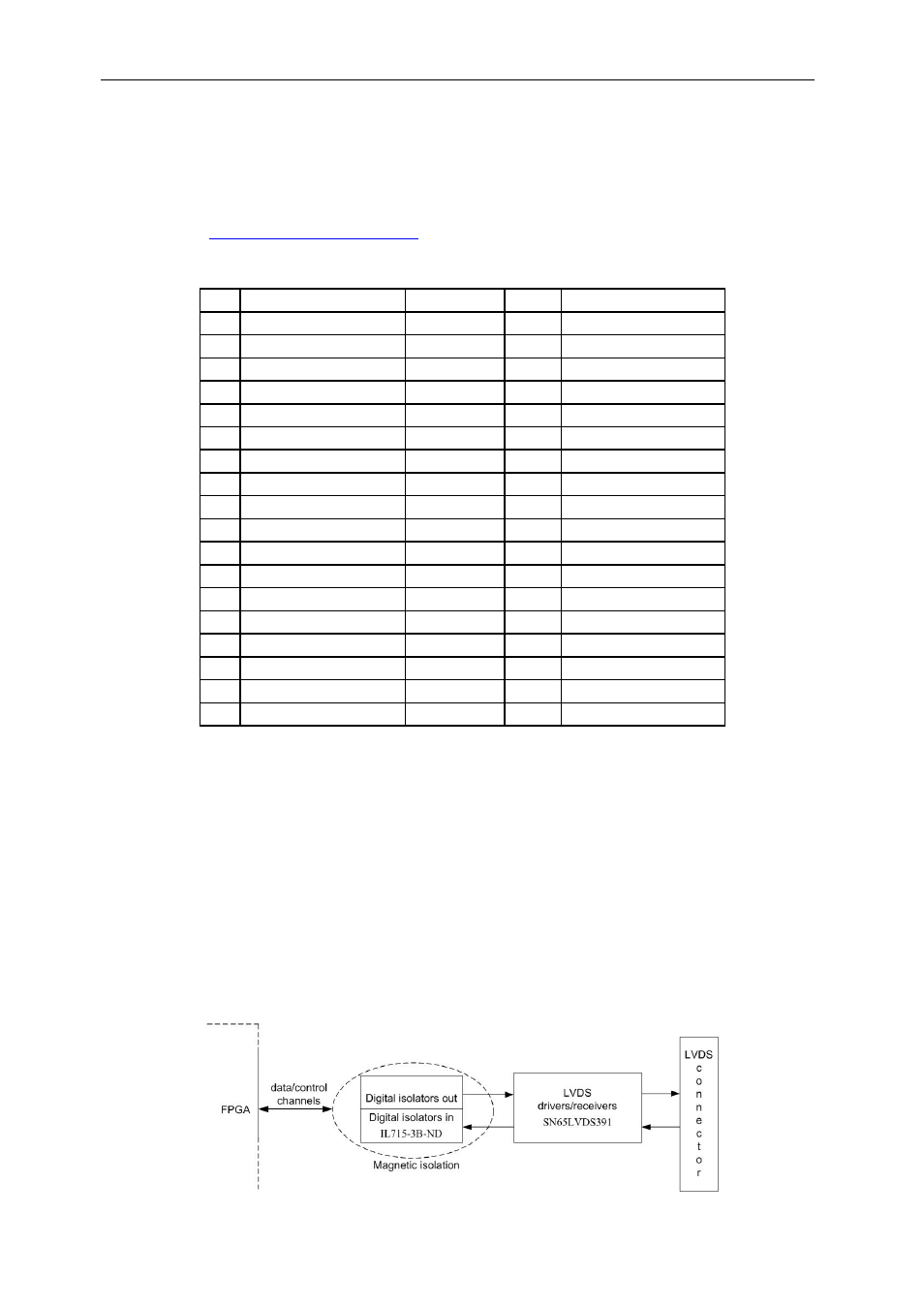
The digital isolators have their own 3.3V power supply with magnetic isolation.
This 4.8Gb/s full duplex link (up to 100Mb/s per differential pair) can be used for
different purposes that require LVDS on the external world for long distance
communications. Data transfers and their associated protocol can be performed and
specifically implemented to meet customers’ requirements (e.g. 4x McBSP channels,
SPI interfaces, interrupts …).
Figure 5 : LVDS circuitry