Debug configurations, Figure 1 - jtag chain, 4 debug configurations – Sundance SMT6012 v.4.6 User Manual
Page 7

Version 4.6
Page 7 of 22
SMT6012 User Manual
4 Debug configurations
The Sundance carrier board includes a JTAG controller chip. This chip enables the
various processor elements on the carrier board to communicate information
between each other.
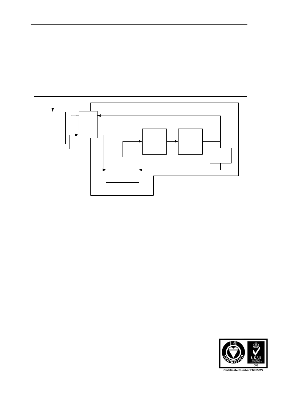
CC and CCS uses the JTAG chain to debug processors. The JTAG chain
interconnects hardware elements as shown in Figure 1 - JTAG Chain.
JTAG Controller
Sundance Carrier Board
DSP 1
DSP 2
TDO
TDI
TDI
TDO
TDO
TDO
TDI
TDI On-
board
TDI Off-
board
External
JTAG chain
TDI
TDO
Off-board
JTAG
connector
On-board
JTAG
connectors
Figure 1 - JTAG Chain
On-board and off-board debugging refers to the way the JTAG chain is used.
For on-board debugging the JTAG chain is local to the carrier board. The JTAG
controller selects the input from the “TDI On-board” pin. This effectively disables
the external JTAG chain.
For Off-board debugging, the JTAG controller chip selects its input from the
external connector. This implies that the JTAG chain now includes the external
JTAG chain. This configuration is useful when you want to debug external
hardware using the carrier board as a master.
If you are connecting the carrier board to other carrier boards located in the same
system, you can use the on-board JTAG connector to make their JTAG paths part
of the JTAG chain of the master carrier board.
Please refer to the user manual of the carrier board that you are using for the
details on how to connect the carrier board with an external JTAG chain.
User Manual (QCF42); Version 4.6, 26/06/02; © Sundance Multiprocessor Technology Ltd. 2002
CCS detects the carrier board with the highest I/O address first. On each of the
carrier boards, the processor in TIM site 1 is detected first and then the processor
on TIM site 2 etc.
