6 i/o address map & register functions, Control registers – Measurement Computing PCM-DAC02 User Manual
Page 12
6 I/O ADDRESS MAP & REGISTER FUNCTIONS
A base address register controls the beginning, or 'Base Address' of the I/O addresses
occupied by the control registers of the PCM-DAC02. Seven addresses are occupied.
The base address assigned by CSS is stored in the CB.CBG file by InstaCal.
CONTROL REGISTERS
After CSS is installed and a base address has been established, the PCM-DAC02 can
be controlled by writing to and reading from the control registers. While it is possible
to write your own control routines for the PCM-DAC02, routines have been written
and are available in Universal library for DOS and Windows programming languages.
NOTE ON REGISTER PROGRAMMING SUPPORT
While the complete register map is explained here, only very limited support for
assembly language or direct register programming is available. Register level
programming should only be done by experienced programmers. We support the use
of the PCM-DAC02 through high level languages using Universal Library.
BASE + 0 - DAC0 LSB Data Register
Any write to this register will trigger an A/D conversion. This is a good method of
starting conversions from software or time-of-day clock control.
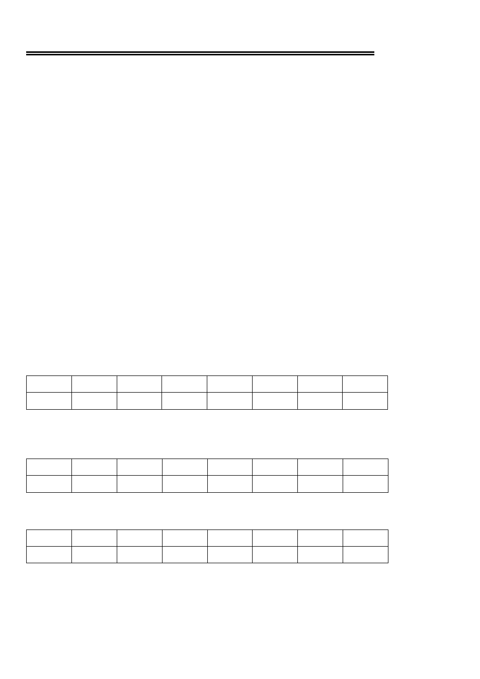
WRITE: D/A Data can be written to this address and to Base + 1 to form a 12-bit
D/A data word.
D/A0
D/A1
D/A2
D/A3
D/A4
D/A5
D/A6
D/A7
0
1
2
3
4
5
6
7
READ: Clears interrupt.
BASE + 1 - DAC0 MSB (4 bits)
WRITE: Send DAC data. & Update outputs of DAC0
D/A8
D/A9
D/A10
D/A11
X
X
X
X
0
1
2
3
4
5
6
7
READ: Calibration: read status (Busy: 0 = busy, 1 = ready)
BUSY
X
X
X
X
X
X
X
0
1
2
3
4
5
6
7
BASE + 2 - DAC1 LSB Data Register
8