Settling time, Digital input / output, Main connector – Measurement Computing PCIM-DAS16JR/16 User Manual
Page 23: Settling time -3, Digital input / output -3, Main connector -3
PCIM-DAS16JR/16 User's Guide
Specifications
Settling time
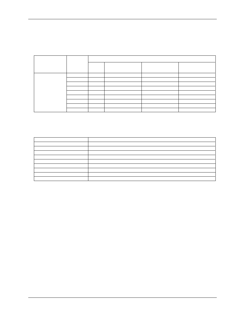
Settling time is defined here as the time required for a channel to settle to within a specified accuracy in
response to a full-scale (FS) step. Two channels are scanned at a specified rate with a –FS DC signal presented
to channel 1 and a +FS DC signal presented to channel 0.
Accuracy
Condition Range
±0.00076%
(±4 LSB)
±0.0015%
(±8 LSB)
±0.0061%
(±16 LSB)
±10 V
Typ.
400 µS
100 µS
10 µS
±5 V
Typ.
100 µS
20 µS
10 µS
±2.5 V
Typ.
60 µS
12 µS
10 µS
±1.25 V
Typ.
50 µS
10 µS
0 to 10 V
Typ.
400 µS
100 µS
10 µS
0 to 5 V
Typ.
100 µS
20 µS
10 µS
0 to 2 V
Typ.
60 µS
12 µS
10 µS
Same range to
same range
0 to 1.25 V
Typ.
50 µS
10 µS
Digital input / output
Main connector
Digital output type
5V/TTL compatible
Digital input type
5V/TTL compatible, pulled to logic high via 10 K resistor network
Number of I/O
8
Configuration
4 fixed input, 4 fixed output
Output high voltage
3.8 volts min. @ -32 mA
Output low voltage
0.55 volts max. @ 32 mA
Input high voltage
2.0 volts min., 7 volts absolute max.
Input low voltage
0.8 volts max., -0.5 volts absolute min.
Data transfer
Programmed I/O
Power-up / reset state
DIG OUT [3:0] - TTL logic low state
6-3