Accuracy, Accuracy -2 – Measurement Computing PCI-DAS6402/16 User Manual
Page 23
PCI-DAS6402/16 User's Guide
Specifications
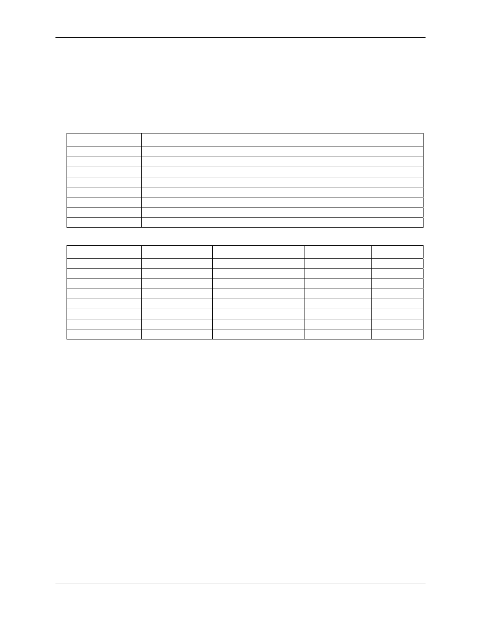
Accuracy
200 kHz sampling rate, single channel operation and a 60 minute warm-up. Accuracies are listed for operational
temperatures within ±2 ºC of internal calibration temperature. Calibrator test source high side tied to Channel 0
High and low side tied to Channel 0 Low. Low-level ground is tied to Channel 0 Low at the user connector.
Table 2. Absolute accuracy
Range Absolute
accuracy
±10.000 V
±3.0 LSB
±5.000 V
±3.0 LSB
±2.500 V
±4.5 LSB
±1.250 V
±4.5 LSB
0 V to +10.000 V
±3.0 LSB
0 V to +5.000 V
±3.0 LSB
0 V to +2.500 V
±4.5 LSB
0 V to +1.250 V
±4.5 LSB
Table 3. Accuracy components
Range
Gain error
Offset error
DLE
ILE
±10.00 V
±1.5 max
±1.5 max
±1.75 max
±2 max
±5.000 V
±1.5 max
±1.5 max
±1.75 max
±2 max
±2.500 V
±2.0 max
±2.5 max
±1.75 max
±2 max
±1.250 V
±2.0 max
±2.5 max
±1.75 max
±2 max
0 to +10.00 V
±1.5 max
±1.5 max
±1.75 max
±2 max
0 to +5.000 V
±1.5 max
±1.5 max
±1.75 max
±2 max
0 to +2.500 V
±1.5 max
±3.0 max
±1.75 max
±2 max
0 to +1.250 V
±1.5 max
±3.0 max
±1.75 max
±2 max
Each PCI-DAS6402/16 is tested at the factory to assure the board’s overall error does not exceed accuracy
limits described in
above.
As shown in Tab
, total analog input error is a combination of gain, offset, differential linearity and integral
linearity error. The theoretical worst-case error of the board may be calculated by summing these component
errors. Worst case errors are realized only in the unlikely event that each of the component errors are at their
maximum level, and causing error in the same direction.
5-2