3 control & data registers – Measurement Computing PC104-DIO48 User Manual
Page 10
3 CONTROL & DATA REGISTERS
We recommend that you use the Universal Library for all high level
programming. The following is basic information on the 82C55 control
and data registers and a table of control bytes for MODE 0 only. To
learn more about the other 82C55 modes, you will need the component
data book available from the component manufacturer.
Each PC104-DIO48 has two 82C55 parallel I/O chips. Each chip
contains three data and one control register occupying four consecutive
I/O address locations. The number of I/O locations occupied by a
PC104-DIO48 board is equal to 4 times the number of 82C55 chips on
the board or eight total.
The first address, or BASE ADDRESS, is determined by setting a bank
of switches on the board.
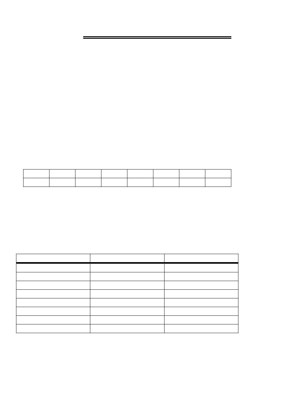
The register descriptions follow all follow the format:
A0
A1
A2
A3
A4
A5
A6
A7
0
1
2
3
4
5
6
7
The numbers along the top row are the bit positions within the 8-bit byte
and the numbers and symbols in the bottom row are the functions
associated with each bit.
To write to or read from a register in decimal or HEX, the bit weights in
Table 2-1 apply:
Table 3-1. Bit Weights
80
128
7
40
64
6
20
32
5
10
16
4
8
8
3
4
4
2
2
2
1
1
1
0
HEX VALUE
DECIMAL VALUE
BIT POSITION
To write a control word or data to a register, the individual bits must be
set to 0 or 1 then combined to form a byte. Data read from registers
must be analyzed to determine which bits are on or off.
6