7 counter timer – Measurement Computing PC104-DAS08 User Manual
Page 17
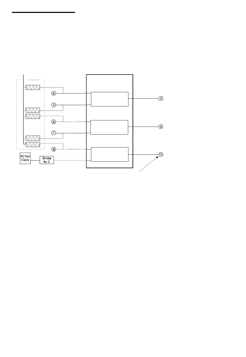
3.7 COUNTER TIMER
The 82C54 counter timer chip can be used for event counting, frequency and pulse
measurement and as a pacer clock for the A/D converter. Several of the Universal
Library A/D routines assume that counter 2, which is hard-wired to the PC bus
signal PCLK, is pacing the A/D samples. All inputs, outputs and gates of the counter
are accessible at the 40 pin analog connector with the exception of the counter 2
input.
Figure 3-1. 82C54 Counter Block Diagram
The primary purpose of the counter timer chip is to pace the A/D samples. The
input to Counter 2 is hard-wired to the PC bus PCLK signal so that a precise timing
signal will always be available on the board. The counter gates, inputs and outputs
are TTL.
The counter GATE2 IN line allows or inhibits TTL level pulses present at the CLK
input into the counter 2 register. The OUT line then transitions (pulses or shifts)
depending on the codes in the control register.
The PCLK signal is divided by two prior to the input at counter 2. Therefore, if the
PCLK signal on your PC/AT is 8 MHz, the signal at the input of counter 2 is 4 MHz.
Assuming a 4 MHz signal at counter 2, the rates out of counter 2 (pin 11) can vary
between 2 MHz (4 MHz / 2) to 61 Hz (4 MHz / 65,535). For rates slower than 61 Hz
the output of counter 2 should be wired to the input of counter 1. The output of
13
CTR2 OUT
CTR1 OUT
CTR0 OUT
GATE0 IN
CTR0 IN
GATE1 IN
CTR1 IN
CTR2 IN
GATE2 IN
82C54
COUNTER
COUNTER 0
COUNTER 1
COUNTER 2
+5VDC
Typ.
ANALOG CONNECTOR
10K