Address switch settings – GAI-Tronics 12593-101 Redundant PPI Switching Module User Manual
Page 3
Pub. 42004-474A
Model 12593-101 Redundant PPI Switching Module
Page 3 of 5
f:\standard ioms - current release\42004 instr. manuals\42004-474a.doc
04/13
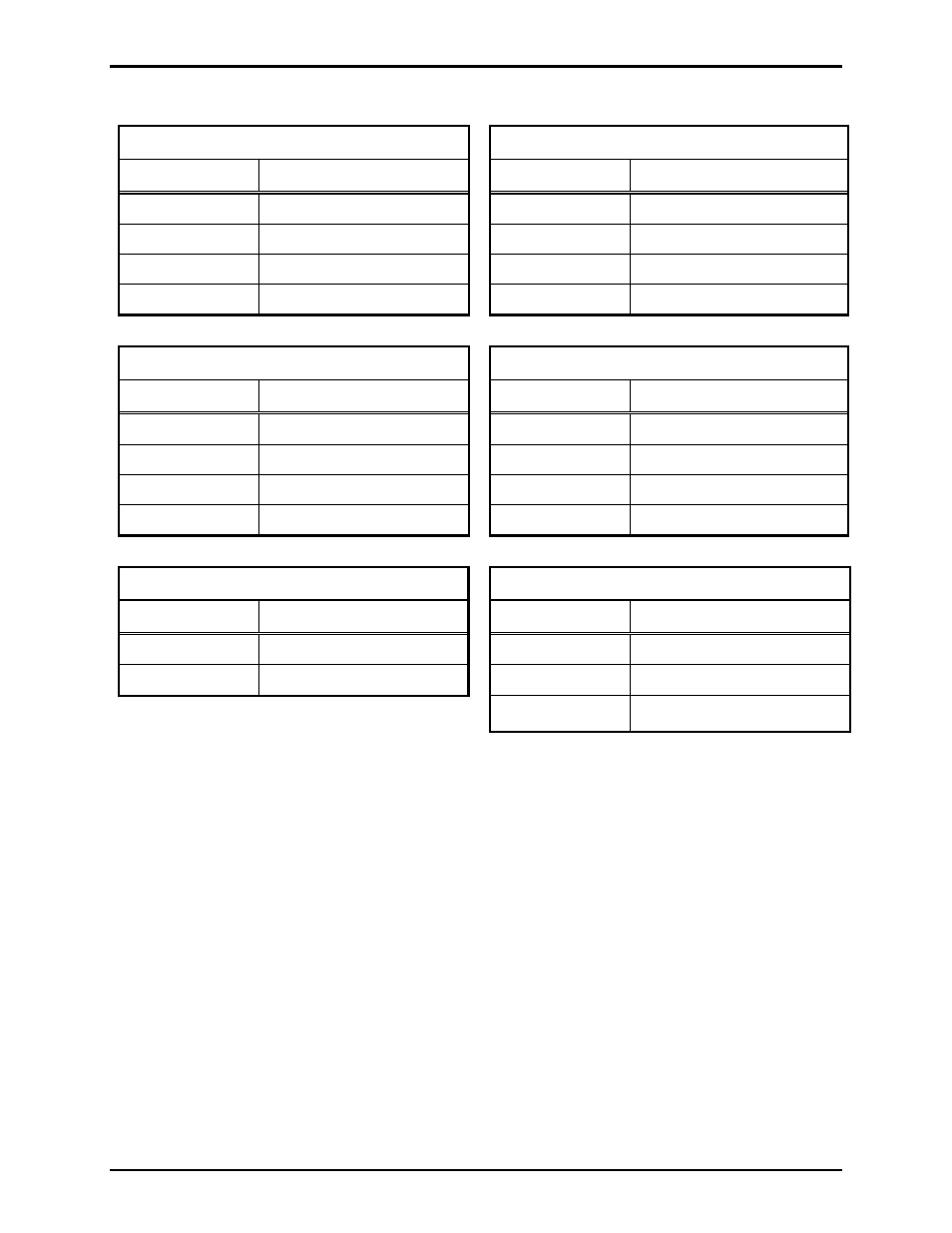
The following is a summary of each connector and terminal block function(s):
J1 – A-IN (RJ45 jack)
J2 – B-IN (RJ45 jack)
Pin No.
Function
Pin No.
Function
1 & 2
Page Line
1 & 2
Page Line
3 & 6
Party Line 1
3 & 6
Party Line 1
4 & 5
Party Line 2
4 & 5
Party Line 2
7 & 8
Control input (CLS)
7 & 8
Control input (CLS)
J3 – OUT (RJ45 jack)
TB1 – 12 V dc Power Input
Pin No.
Function
Terminal No. Function
1 & 2
Page Line
1
12 V (−)
3 & 6
Party Line 1
2
12 V (−)
4 & 5
Party Line 2
3
12 V (+)
7 & 8
Control input (CLS)
4
12 V (+)
TB2 – Switching Control Input
TB3 – Relay Contact Output
Terminal No. Function
Terminal No.
Function
1
Control Line (active low)
1
Normally Close
2
Control Line (active low)
2
Common
3 Normally
Open
Address Switch Settings
Address switches
S1 and S2 on the upper CPU PCBA must each be set to position F
for a board address
of FF. When using multiple modules, address FF must be set on ALL modules. Address FF allows the
module to operate as a Multi-Station Simulator (MSS), with its designated PPI cards. Refer to the
operation section for information on the MSS feature.