Chapter 6 specifications, System block diagram, Connections – Dolby Laboratories DP569 User Manual
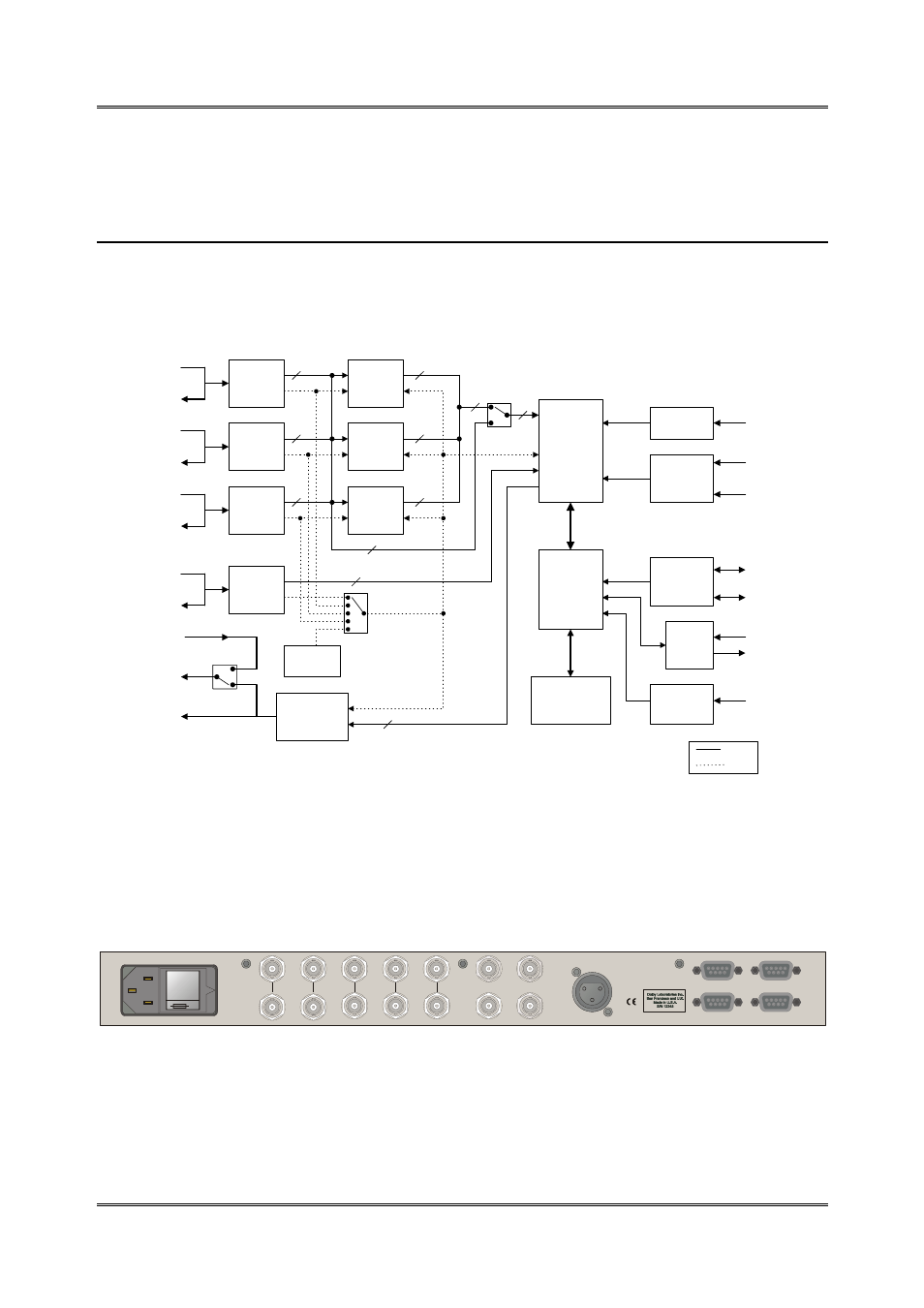
Page 53: 1 system block diagram, 2 connections, Figure 6-1 system block diagram

Model DP569 User’s Manual
6-1
Chapter 6
Specifications
6.1
System Block Diagram
DSP
Processing
Time Code
Rcvr
AES/EBU
Receiver
AES/EBU
Receiver
AES/EBU
Transmitter
Sample
Rate
Converter
µC
Serial
Remote
Control
GPIO
Frame sync
delay
input
User Interface
Front Panel
Local
Clock Ref
Aux Data
SMPTE
LTC In
RS-485
Rear
(RS-422)
Control
AES3
Digital In 3
AES3
Ref In
AES3
Main Out
Front
(RS-232)
AES3 3
Loopthru
AES3 Ref
Loopthru
SMPTE
VITC In
Clock
Reference
Reference
Input
Digital
Input
(32/44.1/48 kHz)
AES3
Switched
Out
Bypass
2
2
6
Status
TTL Pulse
AES3
Bypass In
AES/EBU
Receiver
AES3
Digital In 2
AES3 2
Loopthru
AES/EBU
Receiver
AES3
Digital In 1
AES3 1
Loopthru
Sample
Rate
Converter
Sample
Rate
Converter
6
2
2
2
2
2
2
6
SRC
Select
= clock
= data
Figure 6-1 System Block Diagram
6.2 Connections
CAUTION
To reduce the risk of
fire replace only with
same type and rating
250V slow-blow fuse
100-240 Vac
24VA 50-60Hz
FUSE
T1A
Metadata
Remote
GP I/O In
GP I/O Out
Digital Audio Encoder
Dolby and the double-D symbol are trademarks of Dolby Laboratories Licensing Corporation.
Model DP569
Linear Time
Code In
Main
Switched
Bypass
In
TTL
Out
Delay Out
In 1/2
Dig
Dig
In 3/4
Dig
In 5/6
Ref
In
VITC
In
able parts inside.
WARNING:
No user service-
personnel.
to qualified
Refer all service
WARNING: Check fuse rating before applying power.
Figure 6-2 DP569 Rear Panel
