D table 1 – Zilog EZ80F916 User Manual
Page 11
eZ80F91 Modular Development Kit
User Manual
UM017010-0112
eZ80F91 Module Interface
6
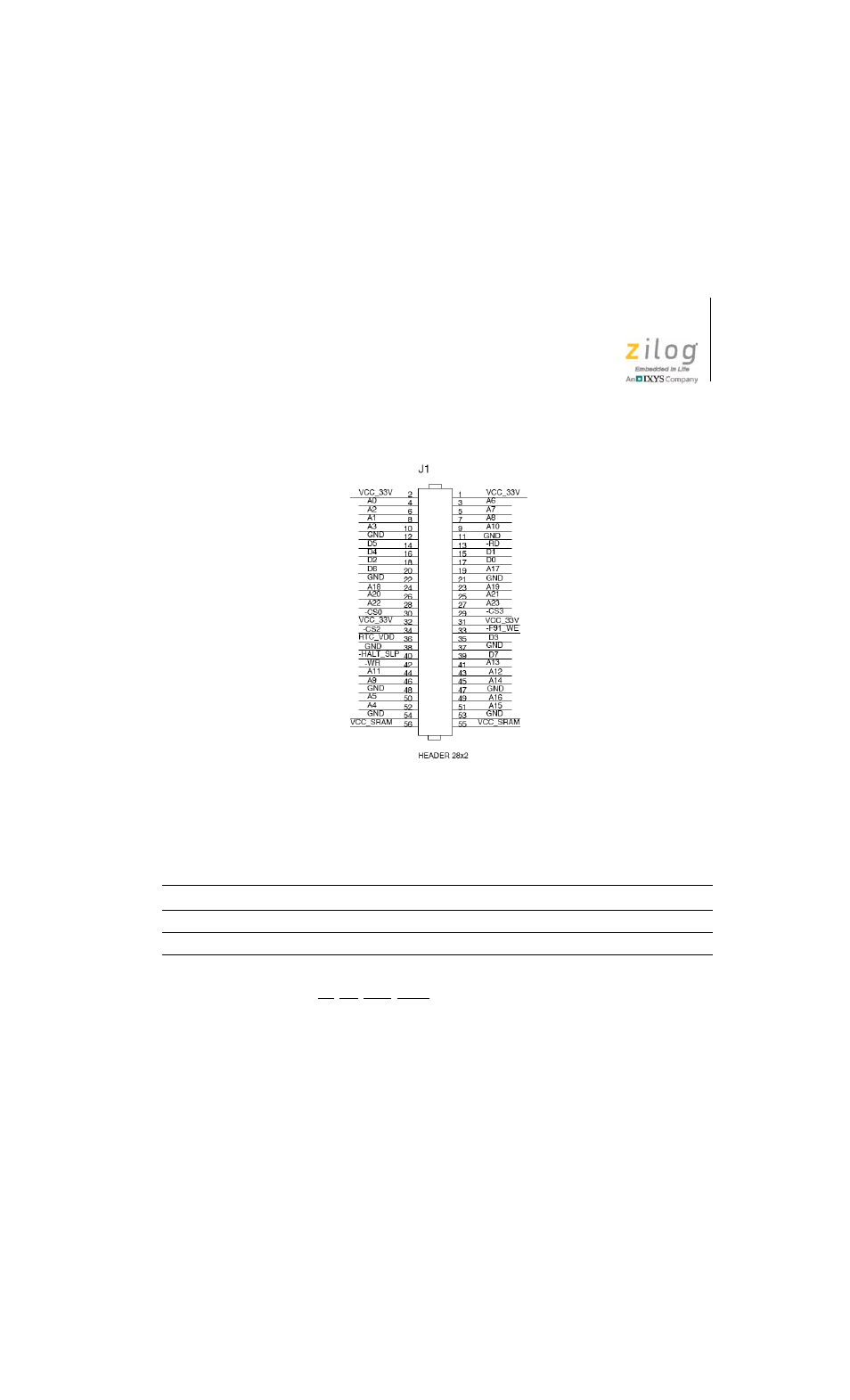
Figure 3. eZ80Acclaim! MDS Adapter Board Peripheral Bus Mini-Module Connector
J1 Pin Configuration
Table 1. eZ80Acclaim! MDS Adapter Board Peripheral Bus Connector J1
Identification
1,2
Pin
Symbol
Signal Direction
Active Level
eZ80F91 Signal
Note
3
A6
Bidirectional
n/a
Yes
4
A0
Bidirectional
n/a
Yes
Notes:
1. To simplify the interface description, Power and Ground nets are omitted from this table. The entire interface
is represented in the eZ80Acclaim! MDS Adapter Board schematics; see Figures 8 and 9.
2. External capacitive loads on RD, WR, IORQ, MREQ, D0–D7 and A0–A23 should be below 10 pF to satisfy the
timing requirements for the eZ80 CPU. All unused inputs should be pulled to either V
DD
or GND, depending on
their inactive levels, to reduce power consumption and to reduce noise sensitivity. To prevent EMI, the EZ80CLK
output can be deactivated via software in the eZ80F91 MCU’s Peripheral Power-Down Register.