Power and ground – ADLINK Express-BE User Manual
Page 25
Express-BE
Page 25
Signal
Pin # Description
I/O
PU/PD
Comment
LID#
A103 LID button. Low active signal used by the ACPI operating system for a LID
switch.
I OD
3.3VSB
PU 10k
3.3VSB
Emulated on
GPIO (BIOS)
SLEEP#
B103 Sleep button. Low active signal used by the ACPI operating system to bring
the system to sleep state or to wake it up again.
I OD
3.3VSB
PU 10K
3.3VSB
Emulated on
GPIO (BIOS)
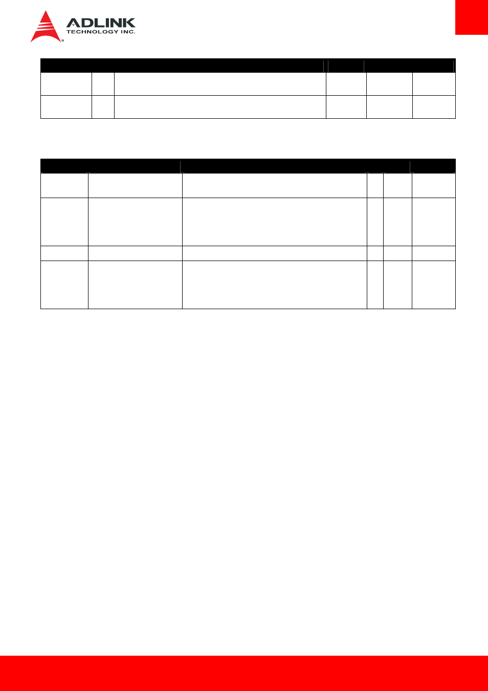
3.3.18. Power and Ground
Signal
Pin #
Description
I/O PU/PD
Comment
VCC_12V A104-A109
B104-B109
Primary power input: +12V nominal (wide range 5 ~ 20V).
All available VCC_12V pins on the connector(s) shall be used.
P
8.5~20
V
VCC_5V_SBY B84-B87
Standby power input: +5.0V nominal. See section 7 “Electrical
Specifications“ for allowable input range. If VCC5_SBY is used,
all available VCC_5V_SBY pins on the connector(s) shall be
used. Only used for standby and suspend functions. May be left
unconnected if these functions are not used in the system design.
P
5Vsb
±5%
VCC_RTC
A47
Real-time clock circuit-power input. Nominally +3.0V.
P
GND
A1, A11, A21, A31, A41, A51,
A57, A66, A80, A90, A96, A100,
A110, B1, B11, B21 ,B31, B41,
B51, B60, B70, B80, B90, B100,
B110
Ground - DC power and signal and AC signal return path.
P