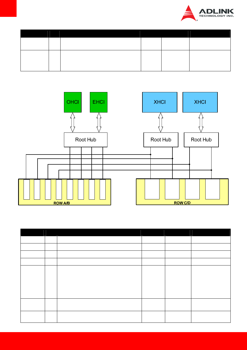
Usb root segmentation, Spi (bios only), Page 22 express-be – ADLINK Express-BE User Manual
Page 22

Page 22
Express-BE
Signal Pin # Description
I/O
PU/PD
Comment
drain driver from a USB current monitor on the carrier
board may drive this line low.
USB_6_7_OC#
A38
USB over-current sense, USB ports 6 and 7. A pull-up
for this line shall be present on the module. An open
drain driver from a USB current monitor on the carrier
board may drive this line low.
I 3.3VSB
PU 10k 3.3VSB
Do not pull high on carrier
3.3.10. USB Root Segmentation
US
B0
- /
A45
US
B0
+
/
A4
6
US
B1
- /
B45
US
B1
+
/
B4
6
US
B2
- /
A42
US
B2
+
/
A4
3
US
B3
- /
B42
US
B3
+
/
B4
3
US
B4
- /
A39
US
B4
+
/
A4
0
US
B5
- /
B39
US
B5
+
/
B4
0
US
B6
- /
A36
US
B6
+
/
A3
7
US
B7
- /
B36
US
B7
+
/
B3
7
US
B_S
S
RX
0
- /
C3
US
B_
S
S
RX
0
+
/
C4
US
B_
S
S
T
X
0
- /
D3
U
S
B_S
S
TX
0+ /
D4
US
B_S
S
RX
1
- /
C6
US
B_
S
S
RX
1
+
/
C7
US
B_
S
S
T
X
1
- /
D6
U
S
B_S
S
TX
1+ /
D7
US
B_S
S
RX
2
- /
C9
US
B_S
S
RX
2
+
/
C10
US
B_
S
S
T
X
2
- /
D9
US
B_
S
S
T
X
2+ /
D10
U
S
B_S
S
RX
3- /
C1
2
US
B_S
S
RX
3
+
/
C13
US
B_
S
S
TX
3
- /
D12
US
B_
S
S
T
X
3+ /
D13
3.3.11. SPI (BIOS only)
Signal
Pin # Description
I/O
PU/PD
Comment
SPI_CS#
B97
Chip select for Carrier Board SPI BIOS Flash.
O 3.3VSB
SPI_MISO
A92
Data in to module from carrier board SPI BIOS flash.
I 3.3VSB
SPI_MOSI
A95
Data out from module to carrier board SPI BIOS flash.
O 3.3VSB
SPI_CLK
A94
Clock from module to carrier board SPI BIOS flash.
O 3.3VSB
SPI_POWER
A91
Power supply for Carrier Board SPI – sourced from Module
– nominally 3.3V.
The Module shall provide a minimum of 100mA on
SPI_POWER.
Carriers shall use less than 100mA of SPI_POWER.
SPI_POWER shall only be used to power SPI devices on
the Carrier
O P 3.3VSB
BIOS_DIS0# A34 Selection
strap to determine the BIOS boot device.
I
PU 10K 3.3VSB
Carrier shall pull to GND
or leave not- connected.
BIOS_DIS1# B88 Selection
strap to determine the BIOS boot device.
I
PU 10K 3.3VSB Carrier shall pull to GND
or leave not- connected
