6 timing signals – ADLINK PXI-2502 User Manual
Page 54

46
• Operation Theoreym
4.6 Timing Signals
In order to meet the requirements for user-specific timing or synchronizing
multiple boards, DAQ/PXI-2500 SERIES provides a flexible interface for
connecting timing signals with external circuitry or other boards. The DAQ
timing of the DAQ/PXI-2500 SERIES is composed of a bunch of counters
and trigger signals in the FPGA on board.
There are 7 timing signals related to the DAQ timing, which in turn influ-
ence the A/D, D/A process, and GPTC operation. These signals are fed
through the Auxiliary Function Inputs pins (AFI) or the System Synchro-
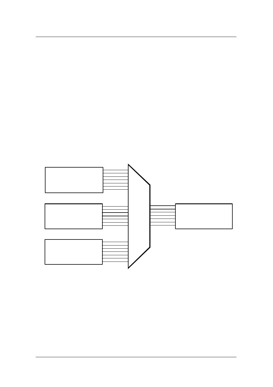
nization Interface bus (SSI). We implemented a multiplexer in the FPGA to
select the desired timing signal from these inputs, as shown in the Figure
4.6.1.
Users can use the SSI to achieve synchronization between multiple boards,
or use the AFI to derive timing signals from an external timing circuit.
Internal timing
signals
SSI timing signals
AFI timing signals
DAQ timing signals
Figure 4.6.1 DAQ signals routing
