Responding functionalities, Figure 4-38: daq signals routing – ADLINK PXI-2006 User Manual
Page 72

62
Operation Theory
20XX series provides flexible user-controllable timing signals to
connect to external circuitry or additional cards.
The whole DAQ timing of the DAQ/PXI-20XX series is composed
of a bunch of counters and trigger signals in the FPGA. These tim-
ing signals are related to the A/D, D/A conversions and Timer/
Counter applications. These timing signals can be inputs to or out-
puts from the I/O connectors, the SSI connector and the PXI bus.
Therefore the internal timing signals can be used to control exter-
nal devices or circuitry’s. Note that in different series of DAQ/PXI-
20XX, the user-controllable timing signals would be slightly differ-
ent. However, the SSI/PXI timing signals remain the same for
every DAQ/PXI-20XX card.
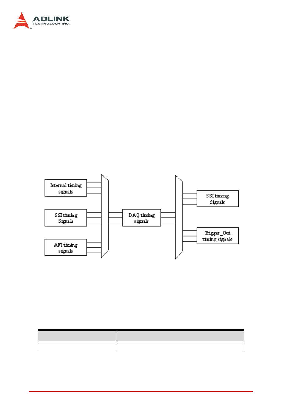
We implemented signal multiplexers in the FPGA to individually
choose the desired timing signals for the DAQ operations, as
shown in the Figure 4-38.
Figure 4-38: DAQ signals routing
Users can utilize the flexible timing signals through our software
drivers, and simply and correctly connect the signals with the
DAQ/PXI-20XX se-ries cards. Here is the summary of the DAQ
timing signals and the corre-sponding functionalities for DAQ/PXI-
20XX series.
Timing signal category
Corresponding functionality
SSI/PXI signals
Multiple cards synchronization
Table 4-8: Summary of user-controllable timing signals and the
corresponding functionalities
