Software update, Is selected) – ADLINK PXI-2006 User Manual
Page 53
Operation Theory
43
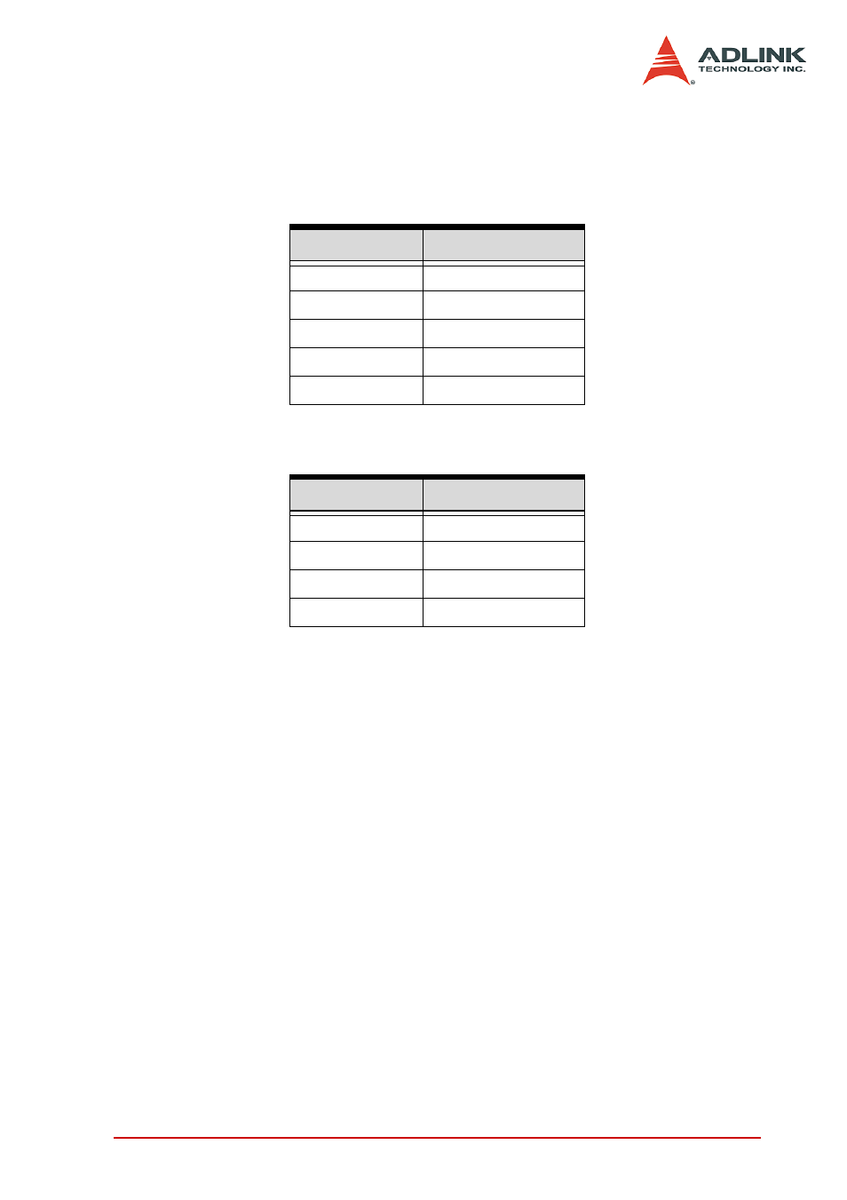
put by feeding a sinusoidal signal into the reference input. The
range of the external reference should be within ±10V. Table 4-5
and 4-6 illustrates the relationship between digital code and output
voltages.
The D/A conversion is initiated by a trigger source. Users must
decide how to trigger the D/A conversion. The data output will start
when a trigger condition is met. Before the start of D/A conversion,
D/A data is transferred from PC’s main memory to a buffering Data
FIFO.
There are two modes of the D/A conversion: Software Update and
Timed Waveform Generation are described, including timing, trig-
ger source con-trol, trigger modes and data transfer methods.
Either mode may be ap-plied to D/A channels independently. You
can software update DA CH0 while generate timed waveforms on
CH1 at the same time.
Software Update
This is the easiest way to generate D/A output. First, users should
specify the D/A output channels, set output polarity: unipolar or
Digital Code
Analog Output
111111111111
Vref * (2047/2048)
100000000001
Vref * (1/2048)
100000000000
0V
011111111111
-Vref * (1/2048)
000000000000
-Vref
Table 4-5: Bipolar output code table (Vref=10V if internal reference is
selected)
Digital Code
Analog Output
111111111111
Vref * (4095/4096)
100000000000 Vref * (2048/4096)
000000000001
Vref * (1/4096)
000000000000
0V
Table 4-6: Unipolar output code table (Vref=10V if internal reference is
selected)