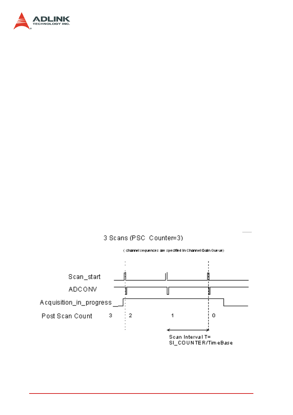
Figure 4-3: scan timing – ADLINK PXI-2006 User Manual
Page 42

32
Operation Theory
pling A/D card, so the “scan interval” equals to the “sampling
interval”.
Example: (Post-trigger acquisition)
Set
SI_counter = 160
PSC_counter = 30
TIMEBASE = Internal clock source
Then
Scan Interval = 160/40M s = 4 us
Total acquisition time = 30 X 4 us = 120 us
TIMEBASE clock source
In scan acquisition mode, all the A/D conversions start on the
output of counters, which use TIMEBASE as the clock source.
By software you can specify the TIMEBASE to be either an
internal clock source (on-board 40MHz clock) or an external
clock input (EXTTIMEBASE) on J5 connector (68-pin VHDCI).
The external TIMEBASE is useful when you want to ac-quire
data at rates not available with the internal A/D sample clock.
The external clock source should generate TTL-compatible
continuous clocks; with a maximum frequency of 40MHz while
the minimum should be 1MHz. Please refer to 4.6 for informa-
tion of user-controllable timing signals.
Figure 4-3: Scan Timing
