0 general description, 1 introduction, 2 test system hardware – Cypress LUPA User Manual
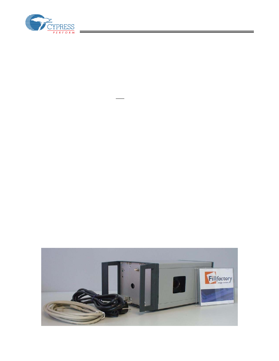
Page 3: 3 multifunctional digital boards, 4 dedicated image sensor board, Figure 1-1. the lupa300 demo kit, Lupa demo kit user guide

LUPA Demo Kit User Guide
Page 3 of 6
1.0
General Description
This guide allows the user to install and run the demo kit properly.
The hardware installation and the software installation are described.
All necessary software and hardware drivers to run the demo kit properly are included on the disk.
Evaluation software (Win 2000 & XP) allows the users to make an evaluation of the LUPA300 sensor and its functionalities.
1.1
Introduction
The LUPA demo kit consists of one multifunctional digital board (memory, FPGA, and ethernet interface) and an analog image
sensor board.
The evaluation software (under Win 2000 or XP; NOT Win 98 or NT), written in HP VEE, allows the grabbing and display of
images and little movies from the sensor. All acquired images and movies can be stored in different file formats. All setting can
be adjusted on the fly to evaluate the sensors specs. Default register values can be loaded to start the software in a desired state.
1.2
Test System Hardware
The test system hardware consists of one multifunctional digital board and an analog image sensor board. These two boards are
connected to an interface backplane and are assembled in a half-rack-width housing. The housing also contains a switching
power supply that allows immediate operation from 220V/110V 50-Hz/60-Hz main power.
1.3
Multifunctional Digital Boards
The demo kit contains one digital board: a multifunctional digital board which has three functionalities: controller (FPGA), memory,
and ethernet interface to the PC.
The digital controller produces the imager timing and supports the computer interface. The controller is made from a Field
Programmable Gate Array (FPGA) that can be reconfigured. During development the FPGA configuration is downloaded via a
parallel download link. Upon delivery of the test system the FPGA configuration is stored in a PROM that is downloaded to the
FPGA at power-on.
The controller contains the logic to produce the clocking signals of the image sensor. It accepts the digital image data and stores
these in the frame memory at nominal operating speed.
The on-board memory (512 MB SDRAM) is used to buffer an imager frame that was grabbed at the nominal read-out frequency.
This stored image will be read out through the Ethernet interface. Both images and little movies can be stored on the SDRAM at
full sensor speed (250 frames/s) and be read out afterwards through the Ethernet interface.
The interface to the PC is standard Ethernet connection. The throughput of this interface is 100 Mbit/s. With some additional
overhead this means we have a resulting full frame rate of 4 images/s on the PC screen.
1.4
Dedicated Image Sensor Board
The dedicated image sensor board contains the power supplies and bias components to support a specific image sensor. In case
of the LUPA300 sensor it contains several power regulators that provide regulated power to the image sensor and its bias circuits.
This power supply is separated from the power supply to the digital controller to avoid interference.
Figure 1-1. The LUPA300 Demo Kit
