Switching characteristics – Cypress CY7C1383DV25 User Manual
Page 19
CY7C1381DV25, CY7C1381FV25
CY7C1383DV25, CY7C1383FV25
Document #: 38-05547 Rev. *E
Page 19 of 28
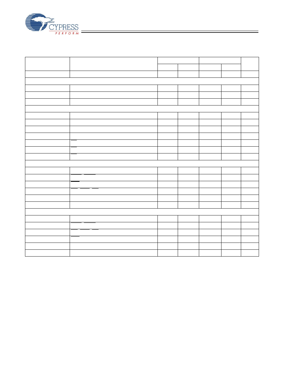
Switching Characteristics
Over the Operating Range
Parameter
Description
133 MHz
100 MHz
Unit
Min.
Max.
Min.
Max.
t
POWER
V
DD
(Typical) to the first Access
1
1
ms
Clock
t
CYC
Clock Cycle Time
7.5
10
ns
t
CH
Clock HIGH
2.1
2.5
ns
t
CL
Clock LOW
2.1
2.5
ns
Output Times
t
CDV
Data Output Valid After CLK Rise
6.5
8.5
ns
t
DOH
Data Output Hold After CLK Rise
2.0
2.0
ns
t
CLZ
Clock to Low-Z
2.0
2.0
ns
t
CHZ
Clock to High-Z
0
4.0
0
5.0
ns
t
OEV
OE LOW to Output Valid
3.2
3.8
ns
t
OELZ
OE LOW to Output Low-Z
0
0
ns
t
OEHZ
OE HIGH to Output High-Z
4.0
5.0
ns
Setup Times
t
AS
Address Setup Before CLK Rise
1.5
1.5
ns
t
ADS
ADSP, ADSC Setup Before CLK Rise
1.5
1.5
ns
t
ADVS
ADV Setup Before CLK Rise
1.5
1.5
ns
t
WES
GW, BWE, BW
[A:D]
Setup Before CLK Rise
1.5
1.5
ns
t
DS
Data Input Setup Before CLK Rise
1.5
1.5
ns
t
CES
Chip Enable Setup
1.5
1.5
ns
Hold Times
t
AH
Address Hold After CLK Rise
0.5
0.5
ns
t
ADH
ADSP, ADSC Hold After CLK Rise
0.5
0.5
ns
t
WEH
GW, BWE, BW
[A:D]
Hold After CLK Rise
0.5
0.5
ns
t
ADVH
ADV Hold After CLK Rise
0.5
0.5
ns
t
DH
Data Input Hold After CLK Rise
0.5
0.5
ns
t
CEH
Chip Enable Hold After CLK Rise
0.5
0.5
ns
Notes
19. Timing reference level is 1.25V.
20. Test conditions shown in (a) of AC Test Loads unless otherwise noted.
21. This part has a voltage regulator internally; t
POWER
is the time that the power needs to be supplied above V
DD
(minimum) initially, before a read or write operation
can be initiated.
22. t
CHZ
, t
CLZ
,t
OELZ
, and t
OEHZ
are specified with AC test conditions shown in part (b) of AC Test Loads. Transition is measured ± 200 mV from steady-state voltage.
23. At any given voltage and temperature, t
OEHZ
is less than t
OELZ
and t
CHZ
is less than t
CLZ
to eliminate bus contention between SRAMs when sharing the same
data bus. These specifications do not imply a bus contention condition, but reflect parameters guaranteed over worst case user conditions. Device is designed
to achieve High-Z prior to Low-Z under the same system conditions.
24. This parameter is sampled and not 100% tested.