Ordering information, Package diagram, Feedback – Cypress CY7C1303BV25 User Manual
Page 18

CY7C1306BV25
CY7C1303BV25
Document #: 38-05627 Rev. *A
Page 18 of 19
© Cypress Semiconductor Corporation, 2006. The information contained herein is subject to change without notice. Cypress Semiconductor Corporation assumes no responsibility for the use
of any circuitry other than circuitry embodied in a Cypress product. Nor does it convey or imply any license under patent or other rights. Cypress products are not warranted nor intended to be
used for medical, life support, life saving, critical control or safety applications, unless pursuant to an express written agreement with Cypress. Furthermore, Cypress does not authorize its
products for use as critical components in life-support systems where a malfunction or failure may reasonably be expected to result in significant injury to the user. The inclusion of Cypress
products in life-support systems application implies that the manufacturer assumes all risk of such use and in doing so indemnifies Cypress against all charges.
Quad Data Rate
™ SRAM and QDR™ SRAM comprise a new family of products developed by Cypress, IDT, NEC, Renesas and
Samsung. All products and company names mentioned in this document may be the trademarks of their respective holders.
Ordering Information
“Not all of the speed, package and temperature ranges are available. Please contact your local sales representative or
visit
www.cypress.com
for actual products offered”.
Speed
(MHz)
Ordering Code
Package
Diagram
Package Type
Operating
Range
167
CY7C1303BV25-167BZC
51-85180 165-ball Fine Pitch Ball Grid Array (13 x 15 x 1.4 mm)
Commercial
CY7C1306BV25-167BZC
CY7C1303BV25-167BZXC
165-ball Fine Pitch Ball Grid Array (13 x 15 x 1.4 mm) Lead free
CY7C1306BV25-167BZXC
CY7C1303BV25-167BZI
165-ball Fine Pitch Ball Grid Array (13 x 15 x 1.4 mm)
Industrial
CY7C1306BV25-167BZI
CY7C1303BV25-167BZXI
165-ball Fine Pitch Ball Grid Array (13 x 15 x 1.4 mm) Lead free
CY7C1306BV25-167BZXI
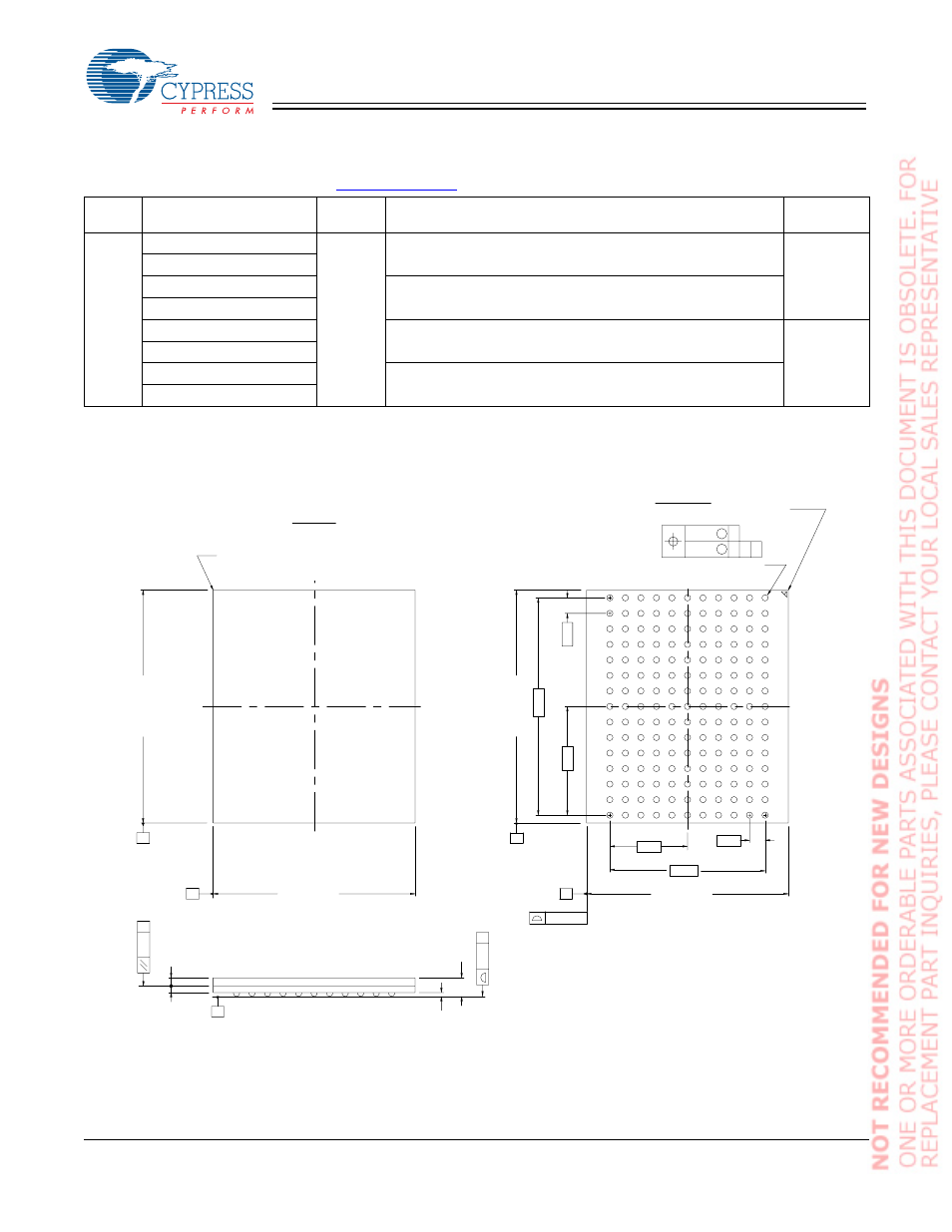
Package Diagram
A
1
PIN 1 CORNER
15.00±0.10
13.00±0.10
7.00
1.00
Ø0.50 (165X)
Ø0.25 M C A B
Ø0.05 M C
B
A
0.15(4X)
0.35±0.06
SEATING PLANE
0.53±0.05
0.25
C
0.15
C
PIN 1 CORNER
TOP VIEW
BOTTOM VIEW
2
3
4
5
6
7
8
9
10
10.00
14.00
B
C
D
E
F
G
H
J
K
L
M
N
11
11
10
9
8
6
7
5
4
3
2
1
P
R
P
R
K
M
N
L
J
H
G
F
E
D
C
B
A
A
15.00±0.10
13.00±0.10
B
C
1.00
5.00
0.36
-0.06
+0.14
1.40
MAX.
SOLDER PAD TYPE : NON-SOLDER MASK DEFINED (NSMD)
NOTES :
PACKAGE WEIGHT : 0.475g
JEDEC REFERENCE : MO-216 / DESIGN 4.6C
PACKAGE CODE : BB0AC
51-85180-*A
165 FBGA 13 x 15 x 1.40 MM BB165D/BW165D
A
1
PIN 1 CORNER
15.00±0.10
13.00±0.10
7.00
1.00
Ø0.50 (165X)
Ø0.25 M C A B
Ø0.05 M C
B
A
0.15(4X)
0.35±0.06
SEATING PLANE
0.53±0.05
0.25 C
0.15 C
PIN 1 CORNER
TOP VIEW
BOTTOM VIEW
2
3
4
5
6
7
8
9
10
10.00
14.00
B
C
D
E
F
G
H
J
K
L
M
N
11
11
10
9
8
6
7
5
4
3
2
1
P
R
P
R
K
M
N
L
J
H
G
F
E
D
C
B
A
A
15.00±0.10
13.00±0.10
B
C
1.00
5.00
0.36
-
0.06
+0.14
1.40 MAX.
SOLDER PAD TYPE : NON-SOLDER MASK DEFINED (NSMD)
NOTES :
PACKAGE WEIGHT : 0.475g
JEDEC REFERENCE : MO-216 / DESIGN 4.6C
PACKAGE CODE : BB0AC
51-85180-*A
165-ball FBGA (13 x 15 x 1.4 mm) (51-85180)
