Digilent Ceres User Manual
Page 3
Ceres Reference Manual
Digilent, Inc.
www.digilentinc.com
® Digilent, Inc.
Page 3
Seven Segment LED display
The Ceres board contains a 4-digit common
anode seven-segment LED display. The
display is multiplexed, which means only seven
cathode signals exist to drive all 28 segments
in the display. Four digit-enable signals drive
the common anodes, and these signals
determine which digit the cathode signals
illuminate.
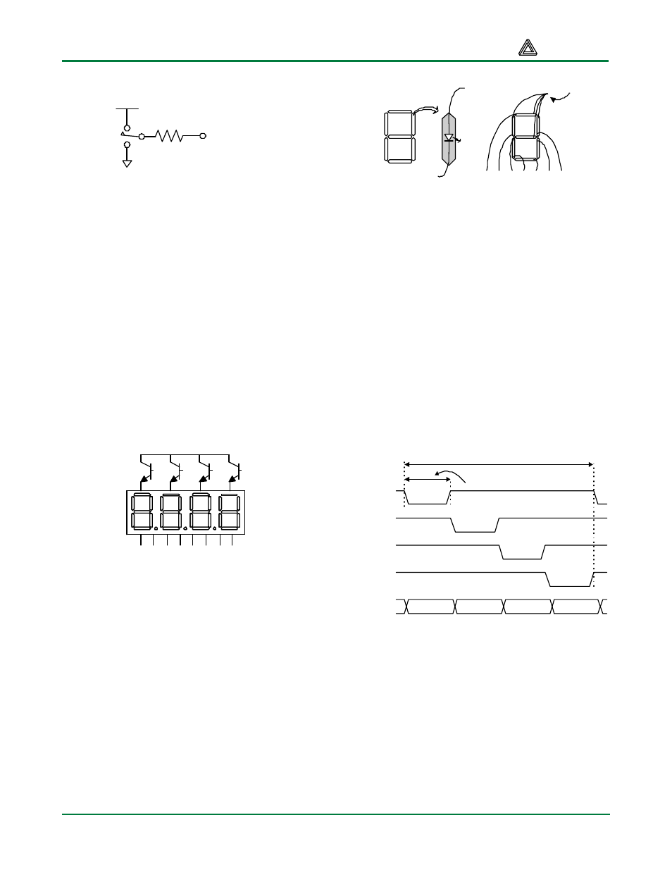
Anodes are connected via
transistors for greater current
Vdd
a b c d e f
g dp
Cathodes are connected to
Xilinx device via 100
Ω
resistors
AN0
AN1
AN2
AN3
Figure 6. Common Anode Sseg display
The seven anodes of each digit’s LEDs are
connected together into one “common anode”
circuit node. The display has four such nodes
named AN0 – AN3, and the signals that drive
these nodes serve as digit enables. Driving an
anode signal low enables the corresponding
digit. The cathodes of similar segments on all
four displays are connected into seven circuit
nodes labeled CA through CG. Driving cathode
signals low illuminates segments on any digit
whose digit enable is low.
Common anode
a
f
e
d
c
b
g
a f g e d c b
Figure 7. Common Anode Detail
This connection scheme creates a multiplexed
display, where driving the anode signals and
corresponding cathode patterns of each digit in
a repeating, continuous succession can create
the appearance of a 4-digit display. Each of the
four digits will appear bright and continuously
illuminated if the digit enable signals are driven
low once every 1 to 16ms (for a refresh
frequency of 1KHz to 60Hz). For example, in a
60Hz refresh scheme, each digit would be
illuminated for ¼ of the refresh cycle, or 4ms.
The controller must assure that the correct
cathode pattern is present when the
corresponding anode signal is driven.
AN0
AN1
AN2
AN3
Digit 0
Refresh period = 1ms to 16ms
Digit period = Refresh / 4
Digit 1
Digit 2
Digit 3
Figure 8. Sseg signal timing
To illustrate the process, if AN0 is driven low
while CB and CC are driven low, then a “1” will
be displayed in digit position 0. Then, if AN1 is
driven low while CA, CB and CC are driven
low, then a “7” will be displayed in digit position
1. If AN0 and CB, CC are driven low for 4 ms,
and then AN1 and CA, CB, CC are driven low
for 4 ms in an endless succession, the display
will show “71” in the rightmost two digits.
GND
Vdd
SW #
signal
4.7K
Ω
Figure 5. Slide Switches