2 i2c interface, 3 i2c address selection, C interface – Digilent 410-287P User Manual
Page 2: C address selection
PmodTMP3 Reference Manual
Copyright Digilent, Inc. All rights reserved.
Other product and company names mentioned may be trademarks of their respective owners.
Page 2 of 3
2 I
2
C Interface
The TCN75AVUA on the PmodTMP3 acts as a slave device using I
2
C serial communication. To communicate with
the PmodTMP3, the master device must specify a slave address (0x48-0x4F) and a flag indicating whether the
communication is a read (1) or a write (0). This is followed by the actual data transfer. For the TCN75AVUA, the
data transfer should consist of the address of the desired device register followed by the data to be written to the
specified register. To read from a register the master must write the desired register address to TCN75AVUA, then
send an I2C restart condition, and send a read request to the TCN75AVUA.
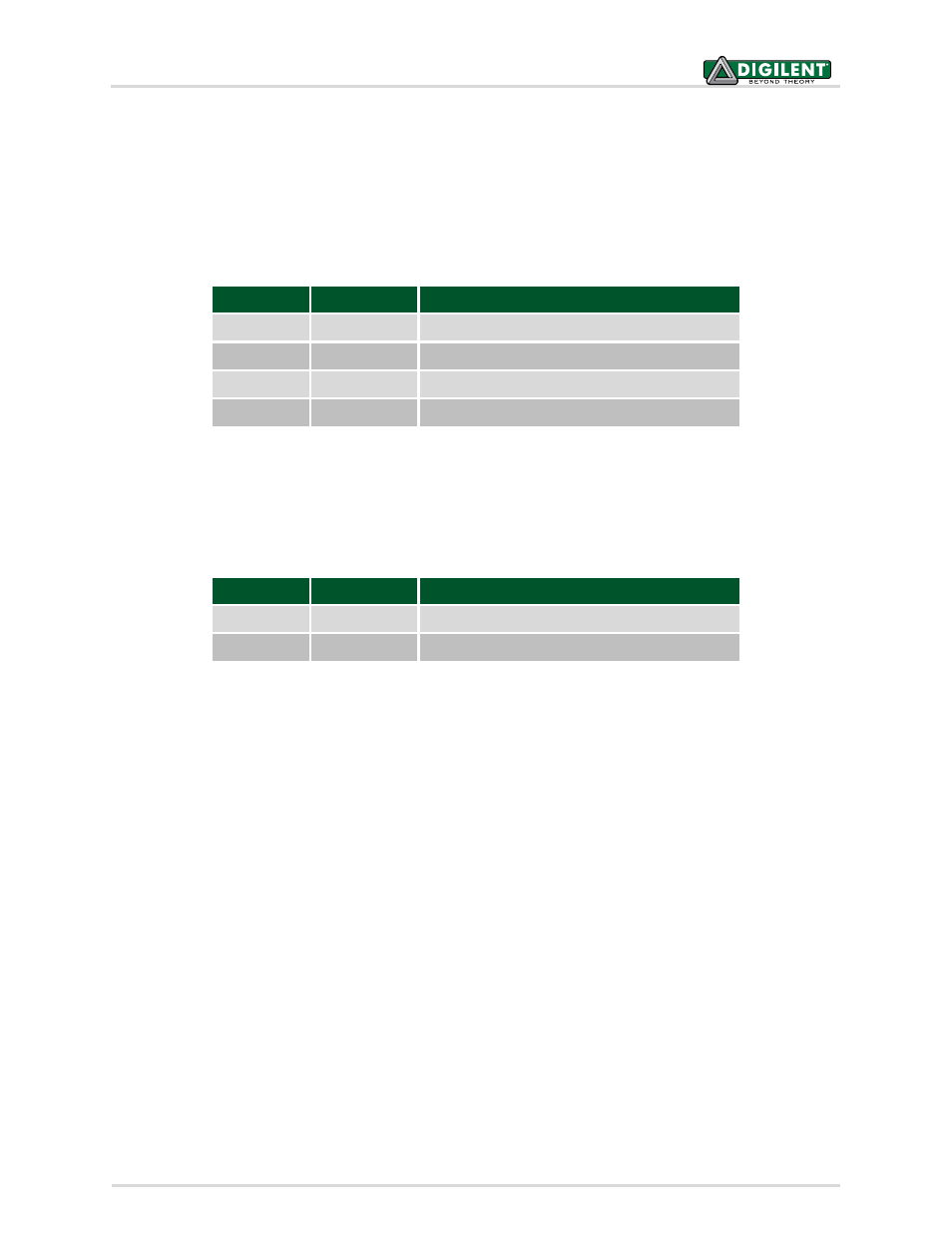
Pin
Signal
Description
1, 2
SCL
I
2
C Clock
3, 4
SDA
I
2
C Data
5, 6
GND
Power Supply Ground
7, 8
3V3
Power Supply (3.3V)
I
2
C Interface Connector Signal Description
The I
2
C interface standard uses two signal lines. These are I
2
C data (SDA) and I
2
C clock (SCL). On the TCN75AVUA,
both SDA and SCL are open-drain pins. For communication to be established, these pins must be connected to pull-
up resistors. The PmodTMP3 has selectable pull-up resistors on jumpers JP4 and JP5. If the master device used to
communicate with the PmodTMP3 does not have pull-up resistors on the SDA and SCL signals, both JP4 and JP5
must be shorted to establish communication via I
2
C. If the master device already has pull-up resistors, these
jumpers may remain open.
JP4
JP5
Pull-Up State
Open
Open
Pull-ups disabled
Shorted
Shorted
Pull-ups enabled
I
2
C Pull-up Jumper Settings
3 I
2
C Address Selection
The PmodTMP3 I
2
C bus can be set to use one of eight valid addresses. The top four bits of the address are fixed,
and the three least significant bits are specified by the states of jumpers JP1, JP2 and JP3. JP1 corresponds to bit
zero of the address, JP2 corresponds to bit one of the address, and JP3 corresponds to bit two of the address. The
address is set by shorting the AX pin on the PmodTMP3 (where X is the bit number) with either 3V3 or GND.
Shorting a jumper in the GND position corresponds to a zero while shorting a jumper in the 3V3 position
corresponds to a one.