Digilent 410-103P-KIT User Manual
Page 2
Document Title
Digilent Confidential
Digilent, Inc.
www.digilentinc.com
Copyright Digilent, Inc.
Page
2
and SCK, serial clock. These signals map to
the following signals on the M25P16 flash
ROM part as described in the ST
Microelectronics data sheet: SS corresponds
to the Chip Select signal, S; MOSI corresponds
to Serial Data Input, D; MISO corresponds to
Serial Data Output, Q; and SCK corresponds
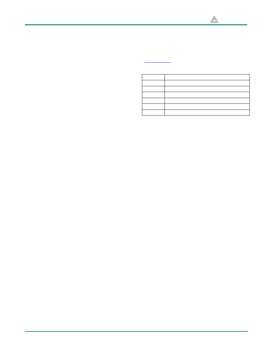
to the Serial Clock signal, C. See Table 1 for a
description of the pins on Pmod interface
connector J1.
The M25P16 flash ROM IC provides additional
inputs called “Hold” and “Write Protect” that are
not used on the PmodSF module. These
signals are held in the inactive state on the
module.
A system board interacts with the PmodSF
module by sending commands over the SPI
interface. Depending on the command sent,
the system board will then send memory data
to, or receive memory data from, the module.
The M25P16 provides commands to perform
sector erase, bulk erase, page program, and
write commands as well as other
miscellaneous commands. Please refer to the
ST Microelectronics data sheet for the M25P16
IC for detailed information on the operation of
this integrated circuit.
The PmodSF is designed to work with either
Digilent programmable logic or Digilent
embedded control system boards. Some
system boards, such as the Nexys, Basys and
Cerebot boards, have 6-pin header connectors
into which the PmodSF will connect directly.
Other Digilent system boards may need a
Digilent Module Interface Board (MIB) and a 6-
pin cable to connect to the PmodSF. The MIB
plugs into the system board and the cable
connects the MIB to the PmodSF.
The PmodSF requires a 3.3V supply voltage.
This power supply voltage is available on all
Digilent system boards and is provided as part
of the 6-wire Pmod interface standard. Digilent
system boards that provide Pmod interface
connectors, allow jumper selection of the
power supply voltage being provided to the
Pmod. Ensure that the system board is
jumpered to provide 3.3V to the module before
applying power to the board.
For detailed information on the M25P16, see
the ST Microelectronics data sheet available at
www.st.com
.
Table 1: Connector J1 Signals
Pin Signal
1 SS
(S)
2 MOSI
(D)
3 MISO
(Q)
4 SCK
(C)
5 GND
6 VCC