Digilent 410-125P User Manual
Page 2
PmodOD1 Reference Manual
Digilent Confidential
Digilent, Inc.
www.digilentinc.com
Copyright Digilent, Inc.
Page
2
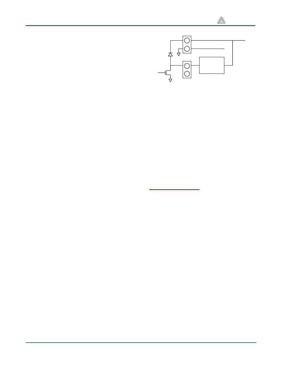
turning the transistor on. The output transistor
will then sink current to ground. Driving an
input low drives the gate of the transistor low,
turning off the output transistor. Each input has
a pull-down resistor that prevents the output
from turning on unless it is actively being
driven high.
Access to the outputs of the PmodOD1 is
provided by screw terminal blocks J2 and J3.
The outputs are labeled OD1 – OD4. Input G1
controls output OD1 and so on. Each output is
connected to the drain of the corresponding
output transistor and functions like a low
impedance switch closure to ground.
Each output provides a clamp diode to prevent
damage due to flyback voltages generated by
inductive loads. Each output transistor
functions independently of the others, so they
can be used individually or simultaneously.
External
Load
J2
or
J3
J4
External Voltage
External Ground
Output
Transistor
Clamp
Diode
ODn
VL
GND
Figure 3 Output Circuit with Load Connection
As illustrated in Figure 3, a load is connected
so that current from an external voltage source
conducts through the load to ground when the
output transistor is turned on. In order to
complete the circuit, the GND pin on J4 must
be connected to the ground for the external
voltage supply. Additionally, the external
voltage source must be connected to the VL
pin on J4 to complete the circuit for the output
clamp diode.
For more information, the PmodOD1
schematic is available at
www.digilentinc.com
.