Digilent 410-270P-KIT User Manual
Digilent Hardware
P
P
m
m
o
o
d
d
A
A
M
M
P
P
3
3
™
™
R
R
e
e
f
f
e
e
r
r
e
e
n
n
c
c
e
e
M
M
a
a
n
n
u
u
a
a
l
l
Revision: February 20, 2013
Note: This document applies to REV A of the board.
1300 NE Henley Court, Suite 3
Pullman, WA 99163
(509) 334 6306 Voice | (509) 334 6300 Fax
Doc: 502-270
page 1 of 2
Copyright Digilent, Inc. All rights reserved. Other product and company names mentioned may be trademarks of their respective owners.
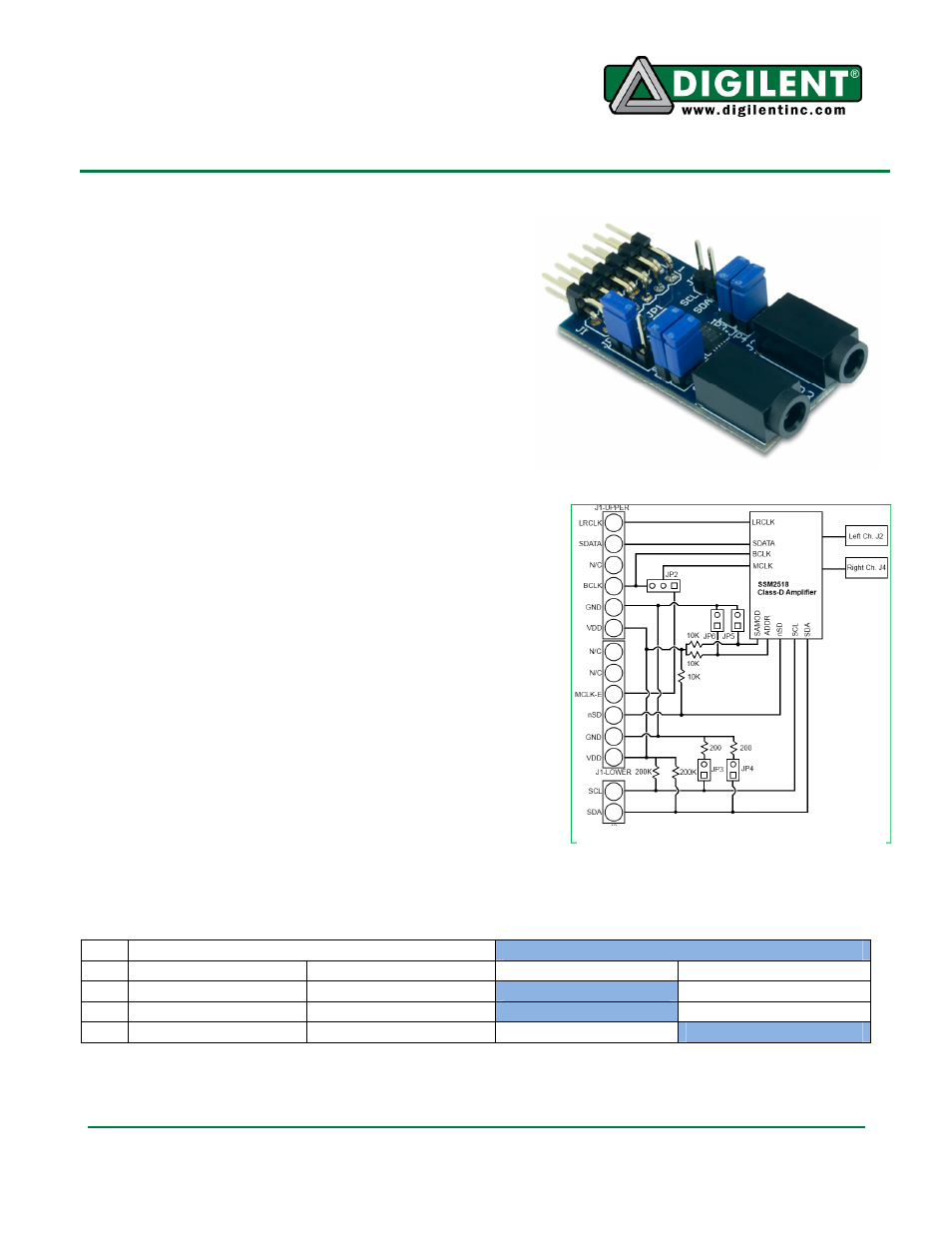
Overview
The Digilent PmodAMP3 features an Analog
Devices SSM2518 2 watt Class-D Audio
Power Amplifier. The module enables the use
of I
2
S audio protocol or TDM to produce stereo
audio at various sampling frequencies. The
module features configurable digital volume
and dynamic range control via an I
2
C interface.
Additionally, you may use the AMP3 in a
stand-alone mode that does not require the
use of the I
2
C interface.
Features Include:
•
separate left and right channel 1/8-inch
headphone jacks
•
12-pin header Pmod™ interface connector
•
supports common I
2
S audio formats
•
digitally configurable volume control for each channel
•
dynamic range control
•
standalone mode for systems without I
2
C interface
•
Operates at 3.3 V
Functional Description
Customers may operate the PmodAMP3 in either an I
2
C
programmable mode or a simple stand-alone mode. The
stand-alone mode is the default setting and can be activated
by clearing the jumper JP5. When the stand-alone mode is
active, the jumpers JP3, JP4, and JP6 allow a simple
hardware configuration of the amplifier. The jumper JP3
configuration determines whether to use Standard or Left
Justified I
2
S protocol. The jumper JP4 determines if the MCLK
input is 256 or 384 times the audio sampling frequency Fs. The jumper JP6 configures the amplifier to
output at either 0dB or +12dB gain. (See Table 1 for further information.)
JP5 Loaded (I
2
C Programmable Mode)
JP5 Unloaded (Stand-Alone Mode)
Loaded
Unloaded
Loaded
Unloaded
JP3 Prohibited
Required
I
2
S (Standard)
Left Justified
JP4 Prohibited
Required
256x Fs
384x Fs
JP6 ADDR: 0110100[r/w]
ADDR: 0110110[r/w]
12dB Gain
0dB Gain
Table 1. Connector Descriptions
Figure 1. Design Layout