Digilent 410-243P User Manual
Page 2
PmodAD5 Reference Manual
www.digilentinc.com
page 2 of 2
Copyright Digilent, Inc. All rights reserved. Other product and company names mentioned may be trademarks of their respective owners.
The PmodAD5 uses the 2.5VDC reference
present on REFIN1+ and REFIN2- by default.
Note: Please see the PmodAD5 schematic,
available from
www.digilentinc.com
, for more
detailed information on GPO and Reference
Supply routing.
Synchronization
Setting the SYNC pin to a logic low puts the
PmodAD5 in a standby state. Once you set the
pin to logic high, the PmodAD5 will begin
gathering samples. The conversion mode
(either single or continuous) must be set
previously.
Bridge Power Down Switch
Operators can use the bridge power down
switch to control external circuitry driving the
analog inputs. Closing this “switch” internally
ties the BPDSW signal to ground.
Analog Supply Voltage
Customers can connect an analog supply
voltage at header J4, if JP1 remains open. You
must keep this external voltage between 3.0V
and 5.25V to avoid damaging your device.
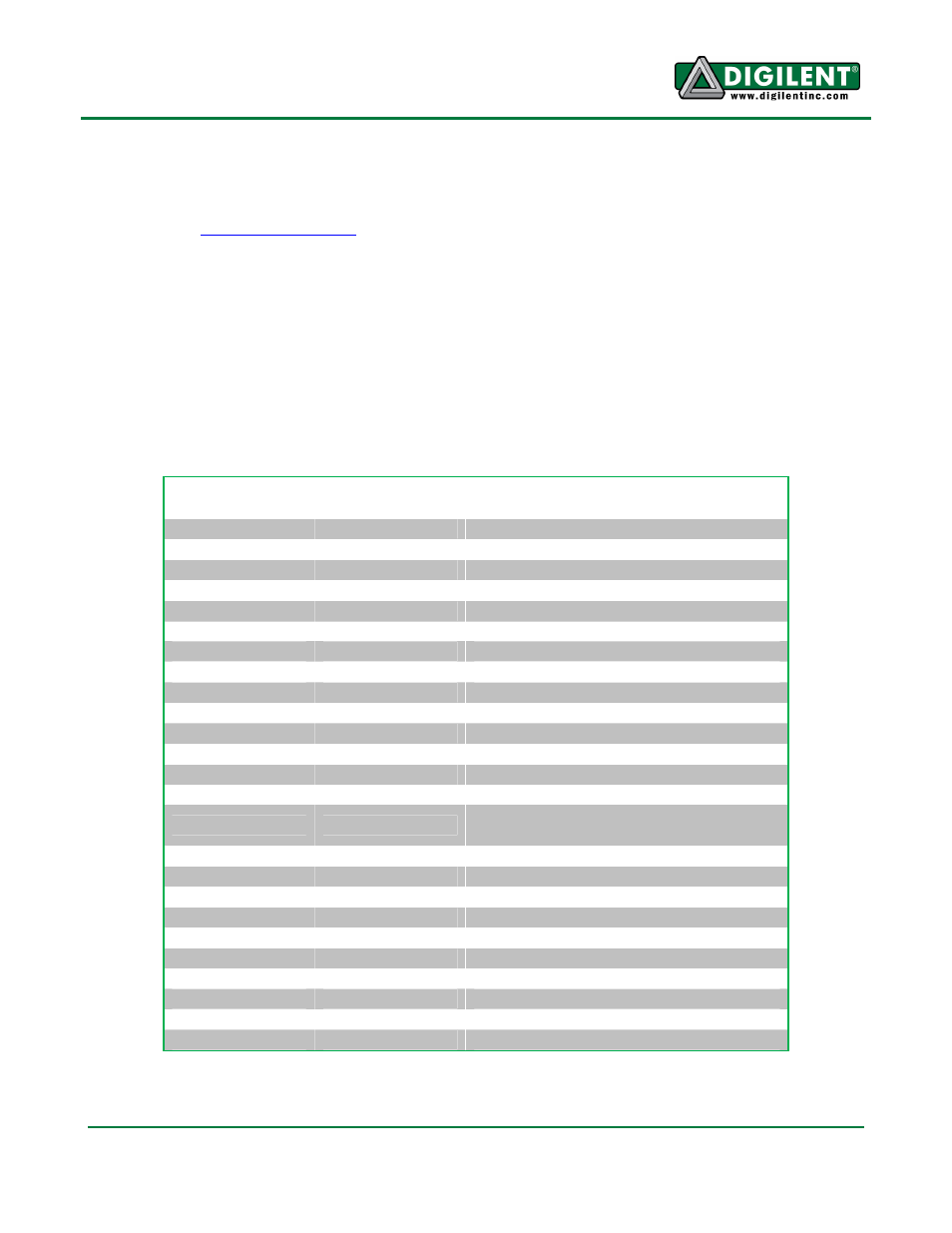
Connector Pin # Pin Name
Description
J1-01
CS
SPI Chip Select. Connect to host ~SS
J1-02
DIN
SPI Data In. Connect to host SDO
J1-03
DOUT/RDY
SPI Data Out. Connect to host SDI
J1-04
SCLK
SPI Clock. Connect to host SCK
J1-05
GND
Ground
J1-06
DVDD
Digital Vdd
J2-01
AIN1
Analog Input 1
J2-02
AIN2
Analog Input 1
J2-03
AIN3
Analog Input 1
J2-04
AIN4
Analog Input 1
J2-05
AIN5
Analog Input 1
J2-06
AIN6
Analog Input 1
J2-07
AIN7
Analog Input 1
J2-08
AIN8
Analog Input 1
J2-09
AINCOM
Analog Input Common, used for
pseudo differential signaling with AIN8:1
J2-10
REFIN2+/P1
Positive Reference Input/GPO1.
J2-11
REFIN2-/P0
Negative Reference Input/GP0.
J2-12
BPDSW
Bridge Power Down Switch.
J3-01
SYNC
Synchronization control
J3-02
P2
GPO2
J3-03
P3
GPO3
J4-01
AVDD
Analog Vdd
J4-02
GND
Ground
J5
AIN1
SMA input 1
J6
AIN2
SMA input 2
Table 1. Connector Pinout Tables