Digilent 410-064P-KIT User Manual
Digilent Hardware

D
D
i
i
g
g
i
i
l
l
e
e
n
n
t
t
P
P
m
m
o
o
d
d
A
A
D
D
1
1
™
™
A
A
n
n
a
a
l
l
o
o
g
g
T
T
o
o
D
D
i
i
g
g
i
i
t
t
a
a
l
l
M
M
o
o
d
d
u
u
l
l
e
e
C
C
o
o
n
n
v
v
e
e
r
r
t
t
e
e
r
r
B
B
o
o
a
a
r
r
d
d
R
R
e
e
f
f
e
e
r
r
e
e
n
n
c
c
e
e
M
M
a
a
n
n
u
u
a
a
l
l
®
w w w . d ig i l en t inc . c om
Revision: December 6, 2011
215 E Main Suite D | Pullman, WA 99163
(509) 334 6306 Voice and Fax
Doc: 502-064
page 1 of 2
Copyright Digilent, Inc. All rights reserved. Other product and company names mentioned may be trademarks of their respective owners.
Overview
The Analog to Digital Module Converter Board
(the AD1™) converts signals at a maximum
sampling rate of one million samples per
second, fast enough for the most demanding
audio applications.
The AD1 uses a 6-pin header connector, and
at less than one square inch is small enough to
be located at the signal source.
Features include:
•
two AD7476A 12-bit A/D converter
chips
•
a 6-pin header connector
•
a 6-pin connector
•
two 2-pole Sallen-Key anti-alias filters
•
two simultaneous A/D conversion
channels at up to one MSa per channel
•
very low power consumption
•
small form factor (0.95” x 0.80”).
Functional Description
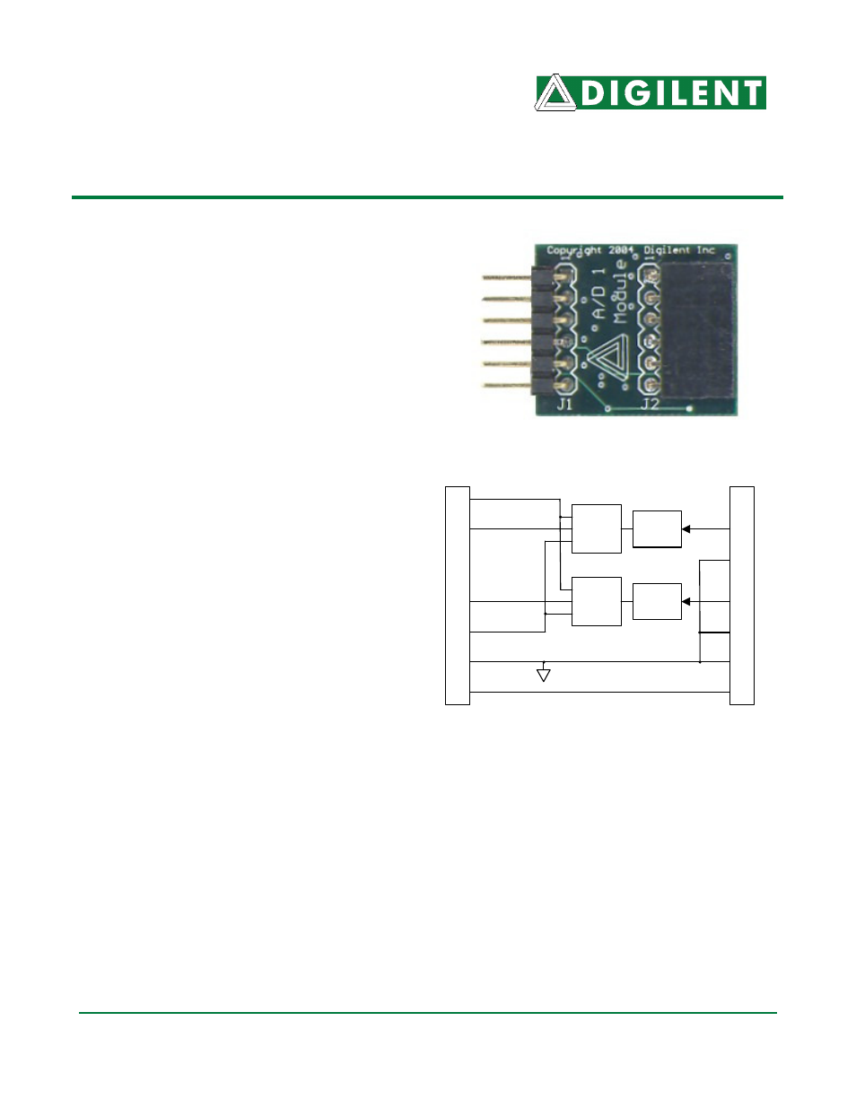
The AD1 converts an analog input signal
ranging from 0-3.3 volts to a 12-bit digital value
in the range 0 to 4095.
The AD1 has two simultaneous A/D conversion
channels, each with a 12-bit converter and
filter. Each channel can sample a separate
stream of analog signals. The AD1 can also
convert a single stream of analog signals using
only one channel.
Each channel has two 2-pole Sallen-Key anti-
alias filters with poles set to 500 KHz. The
filters limit the analog signal bandwidth to a
frequency range suitable to the sample rate of
the converter.
The AD1 uses the SPI/MICROWIRE™ serial
bus standard to send converted data to the
host system. The serial bus can run at up to 20
MHz.
The AD1 has a 6-pin header and a 6-pin
connector for easy connection to a Digilent
system board or other Digilent products.
P3
ADC
1
Filter
Filter
AD1 Circuit Diagram
ADC
2
P4
P2
P1
P1: CS
P2: Data1
P3: Data 2
P4: Clk
P5: GND
P6: Vcc
P5
P6
J2
C
o
n
n
e
ct
o
r
J1
C
o
n
n
e
ct
o
r
