Switching waveforms – Cypress CY7C1318JV18 User Manual
Page 23
CY7C1316JV18, CY7C1916JV18
CY7C1318JV18, CY7C1320JV18
Document Number: 001-15271 Rev. *B
Page 23 of 26
Switching Waveforms
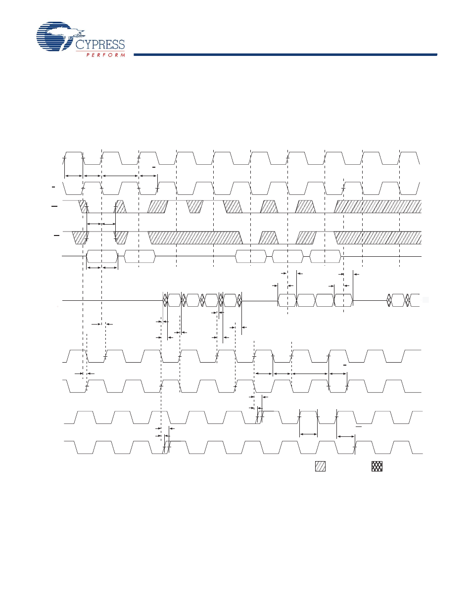
Figure 3. Read/Write/Deselect Sequence
READ
READ
READ
NOP
NOP
WRITE
WRITE
NOP
1
2
3
4
5
6
7
8
9
10
Q40
t
KHCH
tCO
t
tHC
t
tHA
tSD
tHD
tKHCH
tSD
tHD
DON’T CARE
UNDEFINED
tCLZ
tDOH
tCHZ
SC
tKH
tKHKH
tKL
tCYC
A0
D20
D21
D30
D31
Q00
Q11
Q01
Q10
A1
A2
A3
A4
Q41
tCCQO
tCQOH
tCCQO
tCQOH
tKL
tCYC
K
K
LD
R/W
A
DQ
C
C#
CQ
CQ#
SA
tKH
tKHKH
tCQD
tCQDOH
tCQH
tCQHCQH
Notes
24. Q00 refers to output from address A0. Q01 refers to output from the next internal burst address following A0, that is, A0 + 1.
25. Outputs are disabled (High-Z) one clock cycle after a NOP.
26. In this example, if address A2 = A1, then data D20 = Q10 and D21 = Q11. Write data is forwarded immediately as read results. This note applies to the whole diagram.