Write cycle descriptions – Cypress CY7C1268V18 User Manual
Page 10
CY7C1266V18, CY7C1277V18
CY7C1268V18, CY7C1270V18
Document Number: 001-06347 Rev. *D
Page 10 of 27
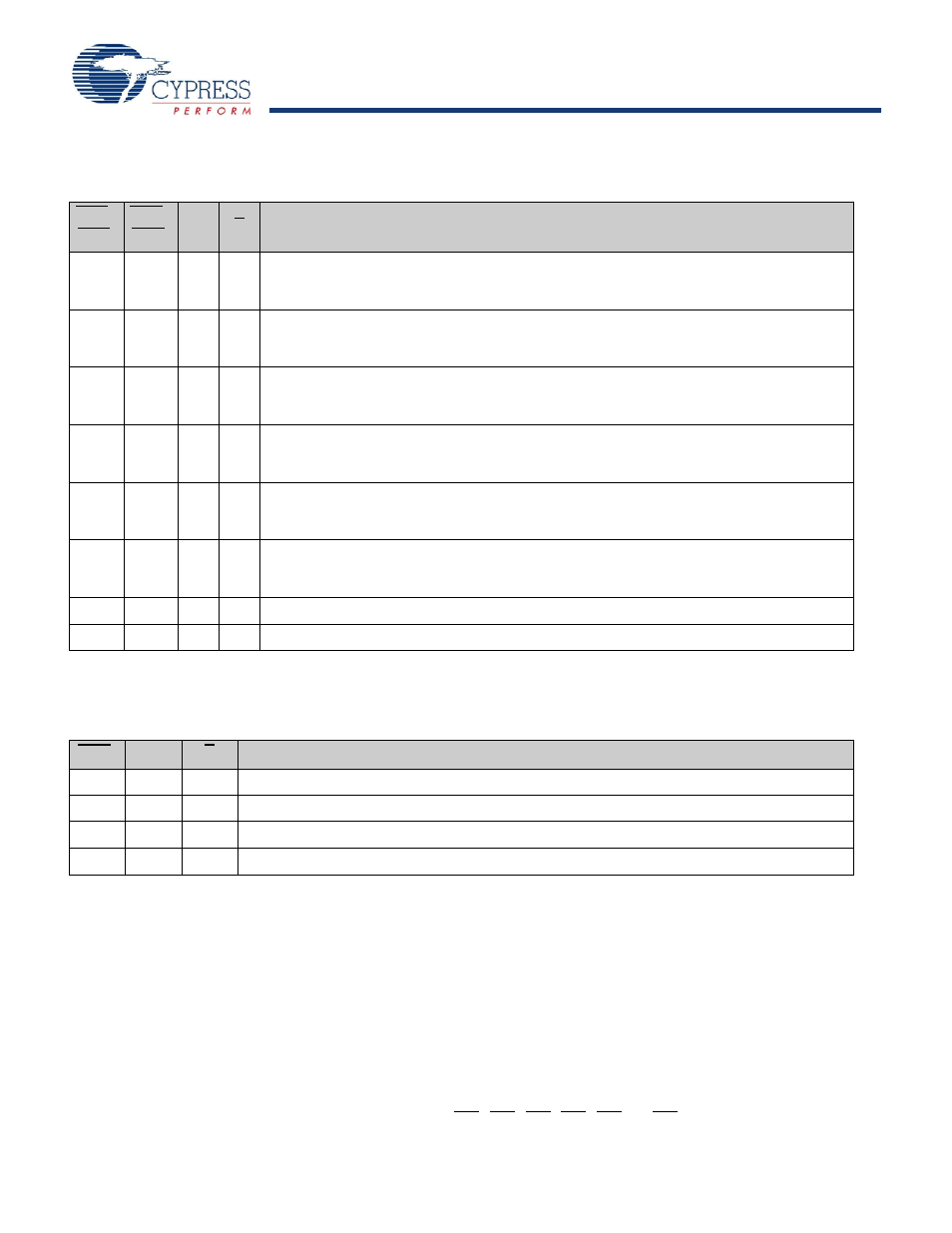
Write Cycle Descriptions
The write cycle description table for CY7C1266V18 and CY7C1268V18 follows.
BWS
0
/
NWS
0
BWS
1
/
NWS
1
K
K
Comments
L
L
L–H
–
During the data portion of a write sequence
:
CY7C1266V18
− both nibbles (D
[7:0]
) are written into the device.
CY7C1268V18
− both bytes (D
[17:0]
) are written into the device.
L
L
–
L-H During the data portion of a write sequence
:
CY7C1266V18
− both nibbles (D
[7:0]
) are written into the device.
CY7C1268V18
− both bytes (D
[17:0]
) are written into the device.
L
H
L–H
–
During the data portion of a write sequence
:
CY7C1266V18
− only the lower nibble (D
[3:0]
) is written into the device, D
[7:4]
remains unaltered.
CY7C1268V18
− only the lower byte (D
[8:0]
) is written into the device, D
[17:9]
remains unaltered.
L
H
–
L–H During the data portion of a write sequence
:
CY7C1266V18
− only the lower nibble (D
[3:0]
) is written into the device, D
[7:4]
remains unaltered.
CY7C1268V18
− only the lower byte (D
[8:0]
) is written into the device, D
[17:9]
remains unaltered.
H
L
L–H
–
During the data portion of a write sequence
:
CY7C1266V18
− only the upper nibble (D
[7:4]
) is written into the device, D
[3:0]
remains unaltered.
CY7C1268V18
− only the upper byte (D
[17:9]
) is written into the device, D
[8:0]
remains unaltered.
H
L
–
L–H During the data portion of a write sequence
:
CY7C1266V18
− only the upper nibble (D
[7:4]
) is written into the device, D
[3:0]
remains unaltered.
CY7C1268V18
− only the upper byte (D
[17:9]
) is written into the device, D
[8:0]
remains unaltered.
H
H
L–H
–
No data is written into the devices during this portion of a write operation.
H
H
–
L–H No data is written into the devices during this portion of a write operation.
Write Cycle Descriptions
The write cycle description table for CY7C1277V18 follows.
BWS
0
K
K
Comments
L
L-H
–
During the data portion of a write sequence
, the single byte (D
[8:0]
) is written into the device.
L
–
L-H
During the data portion of a write sequence
, the single byte (D
[8:0]
) is written into the device.
H
L-H
–
No data is written into the device during this portion of a write operation.
H
–
L-H
No data is written into the device during this portion of a write operation.
Note
8. Assumes a write cycle was initiated per the
tables. NWS
0
, NWS
1
, BWS
0
, BWS
1
, BWS
2
, and BWS
3
can be altered on different portions
of a write cycle, as long as the setup and hold requirements are met.