Xg_lanelinx pin description – Achronix Speedster22i LaneLinx User Manual
Page 8
8
UG035 (v1.0), March 19, 2012
XG_Lanelinx Pin Description
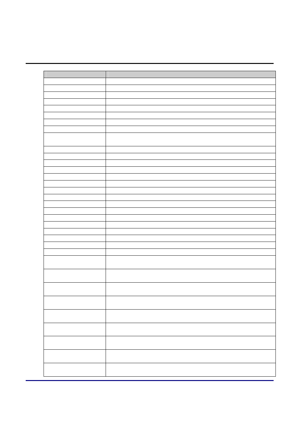
Signal
Description
ref_clk_p
Input. Reference clock p-side (Differential clock-pin)
ref_clk_n
Input. Reference clock n-side (Differential clock-pin)
resetn
Input. Active Low reset line
rx_ch0_p
Input. Serial Data to SerDes p-side
rx_ch0_n
Input. Serial Data to SerDes n-side
tx_data_valid_ch0
Input. Indicates that the input data is valid
tx_sop_ch0
Input. Indicates start-of-packet
tx_eop_ch0
Input. Indicates end-of-packet
tx_err_ch0
Input. Error character must be inserted. At this moment we don’t support
it. It is tied to 1’b0
tx_data_in_ch0[15:0]
Input. Parallel data. Width is 16 bits wide.
tx_valid_bytes_ch0
Input. Number of valid bytes in the data values
tx_ch0_p
Output. Serial Data from SerDes p-side
tx_ch0_n
Output. Serial Data from SerDes n-side
rx_data_out_ch0 [15:0]
Output. Parallel data from rx_data_module block. Width is 16 bits wide.
rx_valid_out_bytes_ch0
Output. Number of valid bytes in data out
rx_data_valid_ch0
Output. Indicates that the output data is valid
rx_sop_ch0
Output. Indicates start-of-packet
rx_eop_ch0
Output. Indicates end-of-packet
rx_err_ch0
Output. Indicates detection of 8b/10b decode or disparity error
tx_ready_ch0
Output. Indicates that bus is ready for data transmission
serdes_tx_clk_ch0
Output. SerDes Transmit clock from the SerDes macro.
serdes_rx_clk_ch0
Output. SerDes Receive clock from the SerDes macro.
MISCELLENEOUS PINS
WILL BE USED FOR ACX Chip-Tap Block for Debugging
debug_bus0[4:0]
Output. Will be used for Chip-Tap debugging tool.
debug_bus1[17:0]
Output. Will be used for Chip-Tap debugging tool.
sig_detect_ch0
Output. ACX SerDes pin which indicates the signal detection. Will be used
in chip-Tap debugging tool.
link_initialized_ch0_tx
Output. Link initialization signal from FSM block. Will be used in Chip-Tap
debugging tool.
rx_data_is_good_ch0
Output. Indicates that the 16-bit data out values are good (no corruption or
error). Will be used in Chip-Tap debugging tool.
rx_switch_data_ch0
Output. Indicates that depending on the SKIP & SYNC character, the 16-bit
will be switched as [{7:0,15:9}]. Will be used in Chip-Tap debugging tool.
rx_skip_ch0
Output. This is to detect SKIP character values of 1C1C pattern. Will be
used in Chip-Tap debugging tool.
rx_sync_ch0
Output. This is to detect SYNC character values of BCBC pattern. Will be
used in Chip-Tap debugging tool.
rx_skip_sync_ch0
Output. This is to detect if there is any combination of 1CBC pattern. Will
be used in Chip-Tap debugging tool.
rx_sync_skip_ch0
Output. This is to detect if there is any combination of BC1C pattern. Will
be used in Chip-Tap debugging tool.
rx_aligned_data_ch0[15:0] Output. This is receiving side aligned data. 16-bit wide. Will be used in
Chip-Tap debugging tool.