Fig. 49 — processor board test points, Fig. 50 — relay board test points – Carrier PC 111 User Manual
Page 49
49
Step 5 — Check Relay Board Outputs from the Processor
Board — This step involves checking the output signals from
relays K1-K3 on the relay board.
1. Turn power to OFF position.
2. Connect negative test probe to TP19 (meter still set to
dc).
3. Turn switch to ON position and enter Quick Test mode.
4. Connect positive test probe to terminal 14 on pin terminal
connector J9, and check voltage from TP19 to terminal
14 on pin terminal connector J9.
5. If not 112 ± 1 vdc, replace processor board.
6. Turn switch to OFF position.
7. Remove negative test probe from TP19. Connect positive
test probe to TP15.
8. Turn switch to ON position and go into Quick Test mode.
9. Place negative lead on terminals shown in Table 24, and
check voltage between TP15 and terminals shown in
Table 23 on pin terminal connector J9. See Fig. 51 for J9
details.
Step 6 — Display Board Connection Checkout
1. Turn power to OFF position.
2. Disconnect the ribbon cable.
3. Connect negative lead of meter to TP18.
4. Turn power to ON position and go into Quick Test mode.
5. Place the other lead on terminals shown in table below,
and check voltage at pin terminals on pin terminal con-
nector J10 (see Fig. 52 for pin terminal connector J10
details):
*Voltage reading is dependent on the meter’s impedance. Readings
may vary with different meters.
PIN TERMINAL
VOLTAGE (DC)
17
5
18
5
20*
2.5
22*
2.5
24
5
K1
K2
K3
C1
C2
C3
C4
C5
C6
C7
C8
CR1
CR2
CR3
CR4
CR5
CR6
CR7
CR8
C27
C15
C14
C26
C25
C24
C23
C22
E3
CR9
CR10
CR11
CR12
CR13
C9
C10
C11
C12
C13
R9
R10
R11
R12
R13
J5
J6
C19
C16
C18
C21
LEGEND
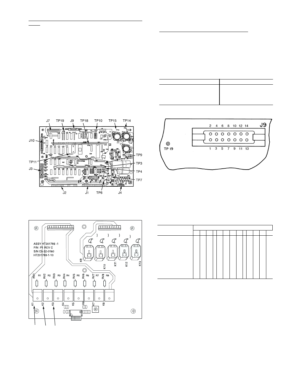
Fig. 49 — Processor Board Test Points
J
— Pin Terminal Strip
TP — Test Pin
LEGEND
Fig. 50 — Relay Board Test Points
CR — Control Relay
J
— Pin Terminal Strip
K
— Relay
Fig. 51 — Relay Board Pin Terminal Connector (J9)
Table 24 — Voltage Reading
NOTES:
1. Pins shown in boldface type will only be energized for 10 seconds.
All other pins will be energized continuously while at the proper
quick test step. The control will only stay in the Quick Test routine
for 10 minutes unless the display button is pressed.
2. Acceptable range for the voltage reading:
0 v — 0 to 4 v
12 v — 11 to 13 v
3. If any of these voltages are not measured, replace the processor
board.
QUICK TEST
STEP NO.
J9 PIN NUMBERS
1
2
3 4 5
6
7
8 9 10 11 12 13
1.-2.3.
0
0
0 0 0
0
0
0 0 0
0
0 12
2.4.
0
0
0 0 0
0 12 0 0 0
0
0 12
2.5.
0
0
0 0 0
0
0 12 0 0
0
0 12
2.6.
0
0
0 0 0
0
0 12 0 12 0
0 12
2.7.
0
0
0 0 0
0
0 12 0 0 12 0 12
2.8.
0
0
0 0 0
0
0 12 0 0
0 12 12
2.9.
12 0
0 0 0
0
0 12 0 0
0
0 12
3.0.
0 12 0 0 0
0
0 12 0 0
0
0 12
3.1.
0
0 12 0 0
0
0 12 0 0
0
0 12
3.2.
0
0
0 0 12 0
0 12 0 0
0
0 12
3.3.
0
0
0 0 0 12 0 12 0 0
0
0 12