Cypress CY7C1034DV33 User Manual
Features, Functional description, Logic block diagram

Cypress Semiconductor Corporation
•
198 Champion Court
•
San Jose
,
CA 95134-1709
•
408-943-2600
Document Number: 001-08351 Rev. *C
Revised January 16, 2009
CY7C1034DV33
6-Mbit (256K X 24) Static RAM
Features
■
High speed
❐
t
AA
= 10 ns
■
Low active power
❐
I
CC
= 175 mA at 10 ns
■
Low CMOS standby power
❐
I
SB2
= 25 mA
■
Operating voltages of 3.3 ± 0.3V
■
2.0V data retention
■
Automatic power down when deselected
■
TTL compatible inputs and outputs
■
Easy memory expansion with CE
1
, CE
2
, and CE
3
features
■
Available in Pb-free standard 119-Ball PBGA
Functional Description
The CY7C1034DV33 is a high performance CMOS static RAM
organized as 256K words by 24 bits. This device has an
automatic power down feature that significantly reduces power
consumption when deselected.
To write to the device, enable the chip (CE
1
LOW, CE
2
HIGH,
and CE
3
LOW) while forcing the Write Enable (WE) input LOW.
To read from the device, enable the chip by taking CE
1
LOW, CE
2
HIGH, and CE
3
LOW, while forcing the Output Enable (OE) LOW
and the Write Enable (WE) HIGH. See the
7 for a complete description of Read and Write modes.
The 24 IO pins (IO
0
to IO
23
) are placed in a high impedance state
when the device is deselected (CE
1
HIGH, CE
2
LOW, or CE
3
HIGH) or when the output enable (OE) is HIGH during a write
operation. (CE
1
LOW, CE
2
HIGH, CE
3
LOW, and WE LOW).
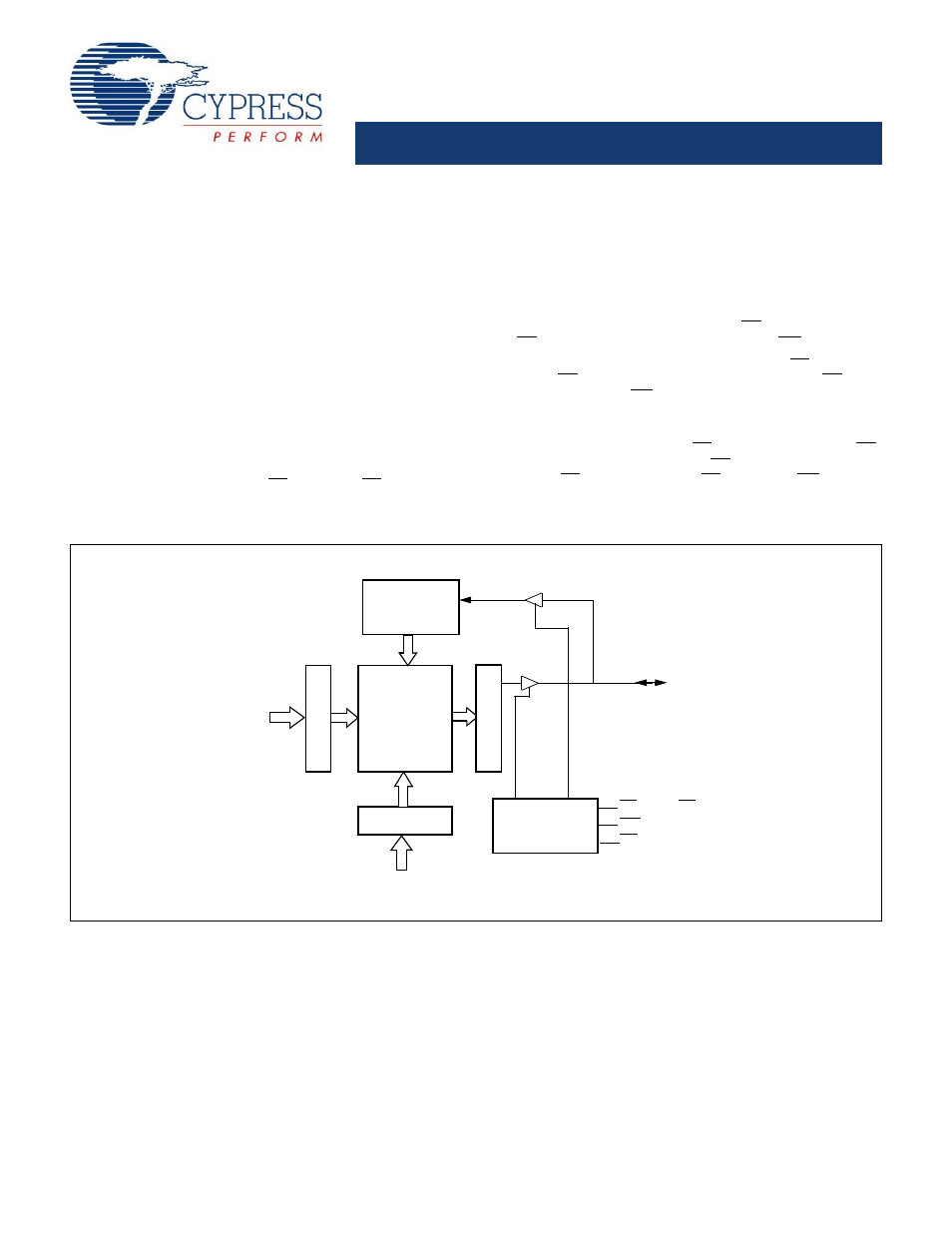
COLUMN
DECODER
ROW DE
CO
DE
R
SE
NSE
AM
PS
INPUT BUFFER
256K x 24
ARRAY
IO
0
– IO
23
OE
CE
1
, CE
2
, CE
3
WE
CONTROL LOGIC
Logic Block Diagram
A
(9:0)
A
(17:10)
Document Outline
- Features
- Functional Description
- Logic Block Diagram
- Selection Guide
- Pin Configuration
- Maximum Ratings
- Operating Range
- DC Electrical Characteristics
- Capacitance
- Thermal Resistance
- AC Switching Characteristics
- Data Retention Characteristics
- Switching Waveforms
- Truth Table
- Ordering Information
- Package Diagram
- Document History Page
- Sales, Solutions, and Legal Information
