Cypress CY7C0251AV User Manual
Features, Logic block diagram

CY7C024AV/024BV/025AV/026AV
CY7C0241AV/0251AV/036AV
3.3V 4K/8K/16K x 16/18 Dual-Port
Static RAM
Cypress Semiconductor Corporation
•
198 Champion Court
•
San Jose
,
CA 95134-1709
•
408-943-2600
Document #: 38-06052 Rev. *J
Revised December 10, 2008
Features
■
True dual-ported memory cells which enable simultaneous
access of the same memory location
■
4, 8 or 16K × 16 organization
■
(CY7C024AV/024BV
/ 025AV/026AV)
■
4 or 8K × 18 organization (CY7C0241AV/0251AV)
■
16K × 18 organization (CY7C036AV)
■
0.35 micron CMOS for optimum speed and power
■
High speed access: 20 and 25 ns
■
Low operating power
❐
Active: I
CC
= 115 mA (typical)
❐
Standby: I
SB3
= 10
μA (typical)
■
Fully asynchronous operation
■
Automatic power down
■
Expandable data bus to 32 bits, 36 bits or more using Master
and Slave chip select when using more than one device
■
On chip arbitration logic
■
Semaphores included to permit software handshaking
between ports
■
INT flag for port-to-port communication
■
Separate upper byte and lower byte control
■
Pin select for Master or Slave (M/S)
■
Commercial and industrial temperature ranges
■
Available in 100-pin Pb-free TQFP and 100-pin TQFP
Notes
1. CY7C024AV and CY7C024BV are functionally identical.
2. IO
8
–IO
15
for x16 devices; IO
9
–IO
17
for x18 devices.
3. IO
0
–IO
7
for x16 devices; IO
0
–IO
8
for x18 devices.
4. A
0
–A
11
for 4K devices; A
0
–A
12
for 8K devices; A
0
–A
13
for 16K devices.
5. BUSY is an output in master mode and an input in slave mode.
R/W
L
OE
L
IO
8/9L
–IO
15/17L
IO
Control
Address
Decode
A
0L
–A
11/12/13L
CE
L
OE
L
R/W
L
BUSY
L
IO
Control
CE
L
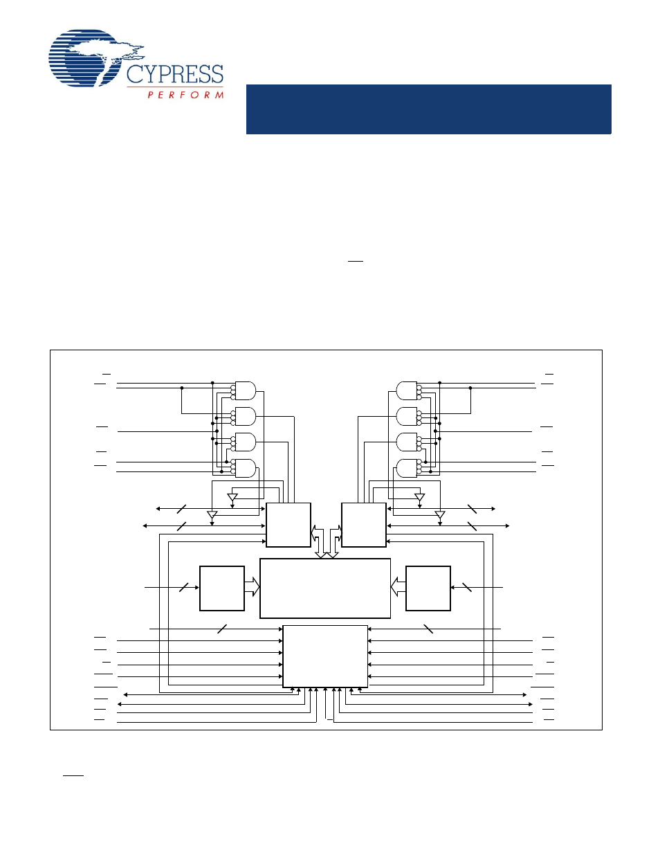
Interrupt
Semaphore
Arbitration
SEM
L
INT
L
M/S
UB
L
LB
L
IO
0L
–IO
7/8L
R/W
R
OE
R
IO
8/9L
–IO
15/17R
CE
R
UB
R
LB
R
IO
0L
–IO
7/8R
UB
L
LB
L
A
0L
–A
11/1213L
True Dual-Ported
RAM Array
A
0R
–A
11/12/13R
CE
R
OE
R
R/W
R
BUSY
R
SEM
R
INT
R
UB
R
LB
R
Address
Decode
A
0R
–A
11/12/13R
[2]
[3]
[3]
[5]
12/13/14
8/9
8/9
12/13/14
8/9
8/9
12/13/14
12/13/14
[4]
[4]
Logic Block Diagram
Document Outline
- Features
- Pin Configurations
- Selection Guide
- Pin Definitions
- Architecture
- Functional Description
- Maximum Ratings
- Operating Range
- Electrical Characteristics Over the Operating Range
- Capacitance
- Switching Characteristics Over the Operating Range [20]
- Data Retention Mode
- Timing
- Switching Waveforms
- Ordering Information
- Package Diagram
- Document History Page
- Sales, Solutions, and Legal Information
