Row b row c, 1794-tbn shown – Rockwell Automation 1794-IF4ICFXT FLEX I/O Isolated Input Analog Module User Manual
Page 3
3
Publication 1794-IN130A-EN-P - December 2009
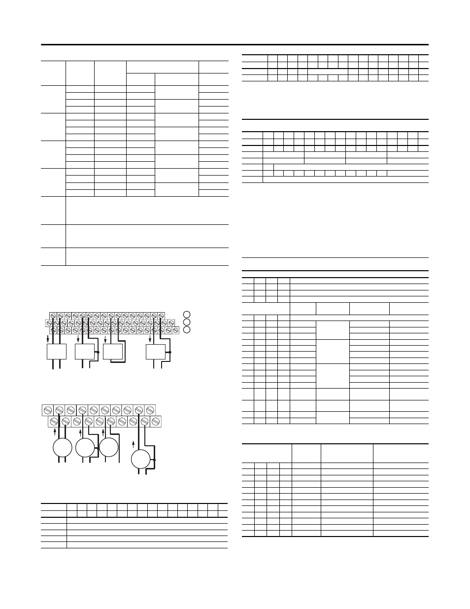
Wire Connections for 1794-IF4ICFXT Modules
7. 1794-TB2, -TB3, and -TB3S - Connect wiring shields to functional
earth ground as near as possible to the module.
1794-TB2, 1794-TB3, 1794-TB3S, 1794-TB3T and 1794-TB3TS Terminal Base
Wiring
1794-TBN Terminal Base Wiring
Input Map
Output Map
Configure Your Input Channels
Input Update Rate for Real Time Sample Interval = 0
Channel
Signal Type
Label
Markings
1794-TB2, -TB3, -TB3S, -TB3T,
-TB3TS
1794-TBN
Terminal
Shield (1794-TB3T,
-TB3TS
Terminal
Input 0
Current
I0
A-0
C-39
B-0
Current
I0 Ret
A-1
C-1
Voltage
V0
A-2
C-40
B-2
Voltage
V0 Ret
A-3
C-3
Input 1
Current
I1
A-4
C-41
B-4
Current
I1 Ret
A-5
C-5
Voltage
V1
A-6
C-42
B-6
Voltage
V1 Ret
A-7
C-7
Output 0
Current
I2
A-8
C-43
B-8
Current
I2 Ret
A-9
C-9
Voltage
V2
A-10
C-44
B-10
Voltage
V2 Ret
A-11
C-11
Output 1
Current
I3
A-12
C-45
B-12
Current
I3 Ret
A-13
C-13
Voltage
V3
A-14
C-46
B-14
Voltage
V3 Ret
A-15
C-15
-V DC
Common
1794-TB2, -TB3, -TB3S - Terminals B-16 through B-33 are internally connected in the terminal
base unit.
1794-TBN - Terminals B-16 and B-33 are internally connected in the terminal base unit.
1794-TB3T, -TB3TS - Terminals 16, 17, 19, 21, 23, 25, 27, 29, 31 and 33 are internally
connected in the terminal base unit.
+V DC
Power
1794-TB3, -TB3S - Terminals 34 through 51 are internally connected in the terminal base unit.
1794-TB3T, -TB3TS - Terminals 34, 35, 50 and 51 are internally connected in the terminal base
unit.
1794-TBN, -TB2 - Terminals 34 and 51 are internally connected in the terminal base unit.
Chassis
Ground
(Shield)
1794-TB3T, -TB3TS - Terminals 39 through 46 are internally connected to chassis ground.
Dec.
15
14
13
12
11
10
9
8
7
6
5
4
3
2
1
0
Oct.
17
16
15
14
13
12
11
10
7
6
5
4
3
2
1
0
Word 0
Analog Value Channel 0
Word 1
Analog Value Channel 1
Word 2
Analog Value Channel 2
Word 3
Analog Value Channel 3
Word 4
Real Time Sample
+
DC only
Current only
+
+
DC only
I
+
A
B
C
+
+
AC or DC
4-Wire Output
Device
+
1
2
3
4
5
6
7
8
9
10
11
12
13 14 15
0
Current
Output
Device
Current
Output
Device
Current
Output
Device
Voltage
Output
Device
I
I
3-Wire Output
Device
2-Wire Output
Device
3-Wire Output
Device
I
_
_
_
_
_
16-33
34-51
0-15
I
R
V
R I
R
V
R
I
R
V
R
I
R
V R
0
1
2
3
4
5
6
7
8
9
10
11
12
16
34
35
36
37
38
39
40
41
42
43
44
45
46
47
48
49
50
51
17
18
19
20
21
22
23
24
25
26
27
28
29
30
33
32
31
13
15
14
16
0
2
4
6
8
10
12
14
33
34
1
3
5
7
9
11
13
15
51
16, 0, 2, 4, 6,
8, 10, 12, 14, 33
34, 1, 3, 5, 7,
9, 11, 13, 15, 51
16
Even Numbered Terminals 0 thru 14
34
Row B
Row C
I
I
+
-
+
-
AC or DC
4-Wire Current
Transmitter
Current
Input
+
DC only
+
+
Current
Input
2-Wire Current
Transmitter
Current only
+
+
Current
Input
+
+
3-Wire
Transmitter
DC only
Voltage
Input
I
I
51
33
1794-TBN shown
3-Wire
Transmitter
Word 5
PU
FP
CF
0
Reserved
0
0
0
0
0
BD
DN
0
Word 6
0
0
0
0
0
0
0
0
V3
V2
V1
V0
U3
U2
U1
U0
Where :
PU = Power up inconfigured
FP = Field power off
CF = In configuration mode
BD = Bad calibration
DN = Calibration accepted
U = Underrange for specified channel
V = Overrange for specified channel
Dec.
15
14
13
12
11
10
9
8
7
6
5
4
3
2
1
0
Oct.
17
16
15
14
13
12
11
10
7
6
5
4
3
2
1
0
Word 0
EN
0
0
0
0
0
0
0
0
0
0
0
0
0
0
0
Word 1
Channel 3 Filter
Channel 2 Filter
Channel 1 Filter
Channel 0 Filter
Word 2
Ch 3 Configuration
Ch 2 Configuration
Ch 1 Configuration
Ch 0 Configuration
Word 3
0
Real Time Sample Interval
Word 4
IC
1
TR
IT
0
CH
SK
FS
RV
QK
CK
GO
Channel Number
Word 5
Reserved
Where :
EN = Enable bit (not used on input module)
IC = Initiate Configuration bit
TR = Transparent bit
IT = Interrupt toggle bit
CH - Chop Mode Disable — use to disable the chop mode. Chop mode used by the module to reduce offset and drift errors. The
default is chop mode enabled (0).
SK = FIR Filter Disable — use to disable the FIR filter. The Finite Impulse Response filter is used by the module to improve signal
stability. The default is FIR filter enabled (0).
FS = Fast Step Response — use to enable a fast step response algorithm. The fast step response algorithm, upon sensing a step
input, uses an averaging method rather than the FIR filter. The FIR goes back into operation once the input has settled. The default is
fast step response disabled (0).
RV = Revert to default bit
QK = Quick calibration
CK = Calibration clock
GO = Gain Offset select
Input Channel Configuration
03
02
01
00
Set these bits for channel 0
07
06
05
04
Set these bits for channel 1
11
10
09
08
Set these bits for channel 2
15
14
13
12
Set these bits for channel 3
Bit Settings
Input Values Data Format
% Underrange
% Overrange
Input Range
0
0
0
0
Channel not configured
0
0
0
1
4…20 mA
signed 2’s
complement
4% under; 4% over
<0000-7878>
0
0
1
0
±10V
2% under; 2% over
<831F-7CE1>
0
0
1
1
±5V
4% under; 4% over
<8618-79E8>
0
1
0
0
0…20 mA
signed 2’s
complement %
0% under; 4% over
<0…10000>
0
1
0
1
4…20 mA
4% under; 4% over
<0…10000>
0
1
1
0
0…10V
0% under; 2% over
<0…10000>
0
1
1
1
±10V
2% under; 2% over
<-10000…10000>
1
0
0
0
0…20 mA
binary
0% under; 4% over
<0000…F3CF>
1
0
0
1
4…20 mA
4% under; 4% over
<0000…F0F1>
1
0
1
0
0…10V
0% under; 2% over
<0000…F9C2>
1
0
1
1
0…5V
0% under; 4% over
<0000…F3CF>
1
1
0
0
±20 mA
offset binary,
8000H = 0 mA
4% under; 4% over
<0618…F9E8>
1
1
0
1
4…20 mA
offset binary,
8000H = 4 mA
4% under; 4% over
<8000…F878>
1
1
1
0
±10V
offset binary,
8000H = 0 mA
2% under; 2% over
<031F…FCE1>
1
1
1
1
±5V
4% under; 4% over
<0618…F9E8>
Configuration Bits
MSD LSD
Input
Nominal
Ranges
Channel Update Rate
(1)
RTSI = 0 and No low
pass filter
Channel Update Rate
RTSI and Filter = 0
IT bit = 1
0
0
0
1
4…20 mA
7.5 ms
5.0 ms
0
0
1
0
±10V
2.5 ms
2.5 ms
0
0
1
1
±5V
2.5 ms
2.5 ms
0
1
0
0
0…20 mA
7.5 ms
5.0 ms
0
1
0
1
4…20 mA
7.5 ms
5.0 ms
0
1
1
0
0…10V
5.0 ms
5.0 ms
0
1
1
1
±10V
5.0 ms
5.0 ms
1
0
0
0
0…20 mA
2.5 ms
2.5 ms
1
0
0
1
4…20 mA
7.5 ms
5.0 ms
1
0
1
0
0…10V
2.5 ms
2.5 ms
1
0
1
1
0…5V
2.5 ms
2.5 ms
1
1
0
0
±20 mA
2.5 ms
2.5 ms
Dec.
15
14
13
12
11
10
9
8
7
6
5
4
3
2
1
0
Oct.
17
16
15
14
13
12
11
10
7
6
5
4
3
2
1
0