Pi33xx-2x i, C digital interface guide – Vicor PI33XX-2X I2C Digital Interface Guide User Manual
Page 14
vicorpower.com Rev 1.0
Cool-Power
®
800 735.6200 11/2012 Page 14 of 22
PI33XX-2X I
2
C Digital Interface Guide
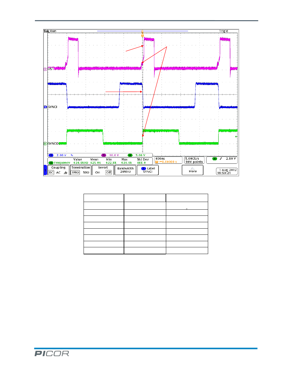
Figure 13 - PI33XX-2X ZVS Buck Sync to T1 Timing Relationship Where VS = Ch3 VS1
SYN[3:0]
SYN[3]
SYN[2:0]
Polarity Bit
Control Bits
SYNC delay
0 = Falling
000
NONE
1 = Rising
001
3/4 MP
100
2/3 MP
101
1/2 MP
110
1/3 MP
111
1/4 MP
Table 5 - PI33XX-2X SYN[3:0] Register Assignments
The ENA_POL and KBIT2 registers are single bit registers. A “0” in the ENA_POL register is the default value. This
means the PI33XX-2X will enable when the ENA pin is floating or logic high. Pulling down ENA pin will disable the
PI33XX-2X. If a “1” is programmed into the ENA_POL register, the ENA polarity reverses. If the ENA pin is floating or
logic low, the PI33XX-2X is enabled. Pulling the ENA pin high will disable the PI33XX-2X.
The KBIT2 register may only be written with a “1” entered into the dialog box. This register can not be read, it is
write only. Burning this register will prevent making any more changes to any register, even if there are unused
bits available to burn.
Start of T1 (ZVS)
Turn on of high side
MOSFET
External sync pulse
falling edge
Start of T1 (ZVS)
Turn on of high side
MOSFET
External sync pulse
falling edge