Data i/o flow and clocking options, Figure 7. cs8420 clock routing – Cirrus Logic CS8420 User Manual
Page 14
14
DS245F4
CS8420
4.
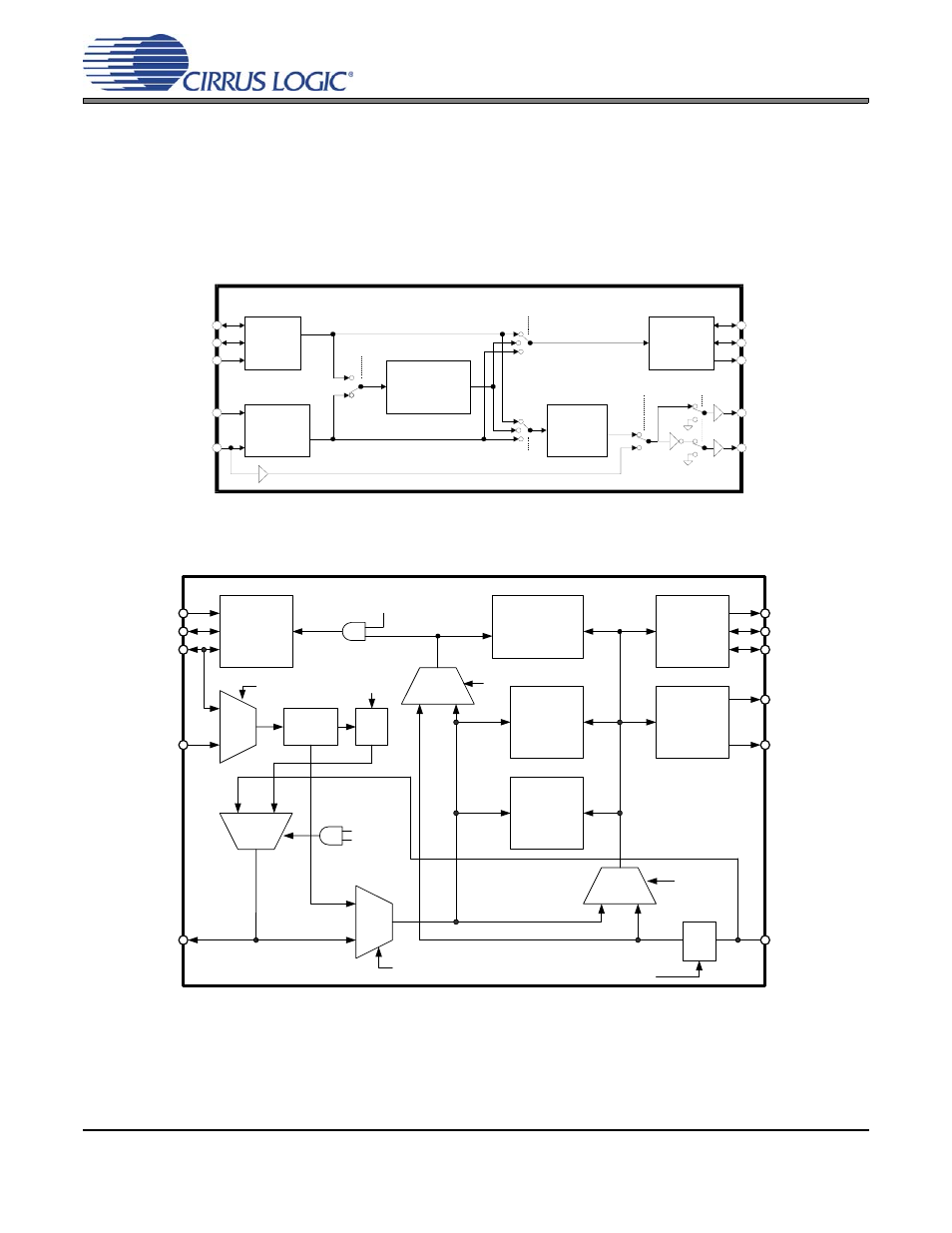
DATA I/O FLOW AND CLOCKING OPTIONS
The CS8420 can be configured for nine connectivity alternatives, referred to as data flows. Each data flow has an
associated clocking set-up.
shows the data flow switching, along with the control register bits which control
the switches. This drawing only shows the audio data paths for simplicity.
shows the internal clock routing
and the associated control register bits. The clock routing constraints determine which data routing options are ac-
tually usable.
Serial
Audio
Input
AES3
Encoder
Serial
Audio
Output
Receiver
Sample
Rate
Converter
RXP
RXN
ILRCK
ISCLK
SDIN
OLRCK
OSCLK
SDOUT
TXP
TXN
AES3
TXOFF
AESBP
SPD1-0
TXD1-0
SRCD
Figure 6. Software Mode Audio Data Flow Switching Options
SIMS
PLL
TXP
TXN
SDOUT
OSCLK
OLRCK
OMCK
RMCK
RXP
ILRCK
ISCLK
SDIN
MUX
MUX
MUX
SWCLK
UNLOCK
0
1
0
1
0
1
CHANNEL
STATUS
MEMORY
USER
BIT
MEMORY
TRANSMIT
AES3
SERIAL
AUDIO
OUTPUT
INC
RXD0
MUX
0
1
OUTC
SERIAL
AUDIO
INPUT
RXD1
MUX
0
1
÷
CLK[1:0]
÷
RMCKF
SAMPLE
RATE
CONVERTER
Figure 7. CS8420 Clock Routing
*Note: When SWCLK mode is enabled, signal input on OMCK is only output through RMCK and not
routed back through the RXD1 multiplexer; RMCK is not bi-directional in this mode.